
Manual


10
4912C–AUTO–10/06
ATA6827 [Preliminary]
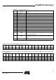
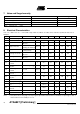
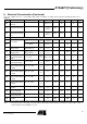
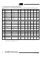
4.13
High-side output switch
on delay
(1)
V
VS
= 13V
R
Load
= 30Ω
t
don
20 µs A
4.14
Low-side output switch
on delay
(1)
V
VS
= 13V
R
Load
= 30Ω
t
don
20 µs A
4.15
High-side output switch
off delay
(1)
V
VS
= 13V
R
Load
= 30Ω
t
doff
20 µs A
4.16
Low-side output switch
off delay
(1)
V
VS
= 13V
R
Load
= 30Ω
t
doff
3µsA
4.17
Dead time between
corresponding high-
and low-side switches
V
VS
= 13V
R
Load
= 30Ω
t
don
– t
doff
1 µs A
5 Logic Inputs DI, CLK, CS, INH
5.1
Input voltage low-level
threshold
3, 4, 5,
8
V
IL
0.3 ×
V
VCC
V A
5.2
Input voltage high-level
threshold
3, 4, 5,
8
V
IH
0.7 ×
V
VCC
V A
5.3
Hysteresis of input
voltage
3, 4, 5,
8
∆V
I
50 700 mV B
5.4
Pull-down current pin
DI, CLK, INH
V
DI
, V
CLK,
V
INH
= V
CC
4, 5, 8 I
PD
5 70 µA A
5.5
Pull-up current
Pin CS
V
CS
= 0V 3 I
PU
–70 –5 µA A
6 Serial Interface – Logic Output DO
6.1 Output-voltage low level I
DOL
= 2 mA 7 V
DOL
0.4 V A
6.2
Output-voltage high
level
I
DOL
= –2 mA 7 V
DOH
V
VCC
–0.7V
V A
6.3
Leakage current
(tri-state)
V
CS
= V
CC
0V < V
DO
< V
VCC
7 I
DO
–15 +15 µA A
7 Inhibit Input - Timing
7.1
Delay time from
standby to normal
operation
t
dINH
100 µs A
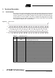
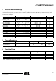
8. Electrical Characteristics (Continued)
7.5V < V
VS
< 40V; 4.75V < V
VCC
< 5.25 V; INH = High; –40°C ≤ T
j
≤ 200°C; T
a
≤ 150°C; unless otherwise specified, all values refer to
GND pins.
No. Parameters Test Conditions Pin Symbol Min. Typ. Max. Unit Type*
*) Type means: A =100% tested, B = 100% correlation tested, C = Characterized on samples, D = Design parameter
Note: 1. Delay time between rising edge of the input signal at pin CS after data transmission and switch on output stages to 90% of
final level. Device not in standby for t > 1 ms