
User guide

87
ATA5811/ATA5812 [Preliminary]
4689B–RKE–04/04
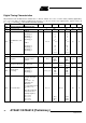
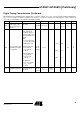
17.9
PWR_H input
-Low level input voltage
9 V
Il
0.25 V A
-Input current low 9 I
Il
-5 µA A
-High level input voltage 9 V
Ih
1.7 AVCC V A
-Input current high 9 I
Ih
1 µA A
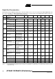
17.10
SDO_TMDO output
-Saturation voltage low
V
VSINT
= 2.4 V to 5.25 V
I
SDO_TMDO
= 250 µA
31 V
ol
0.15 0.4 V B
Saturation voltage high
V
VSINT
= 2.4 V to 5.25 V
I
SDO_TMDO
= -250 µA
31 V
oh
V
VSINT
-
0.4
V
VSINT
-
0.15
V B
17.11
IRQ output
-Saturation voltage low
V
VSINT
= 2.4 V to 5.25 V
I
IRQ
= 250 µA
29 V
ol
0.15 0.4 V B
Saturation voltage high
V
VSINT
= 2.4 V to 5.25 V
I
IRQ
= -250 µA
29 V
oh
V
VSINT
-
0.4
V
VSINT
-
0.15
V B
17.12
CLK output
-Saturation voltage low
V
VSINT
= 2.4 V to 5.25 V
I
CLK
= 100 µA
internal series resistor
of 1 kΩ for spurious
reduction in PLL
30 V
ol
0.15 0.4 V B
Saturation voltage high
V
VSINT
= 2.4 V to 5.25 V
I
CLK
= -100 µA
internal series resistor
of 1 kΩ for spurious
reduction in PLL
30 V
oh
V
VSINT
-
0.4
V
VSINT
-
0.15
V B
17.13
N_RESET output
-Saturation voltage low
V
VSINT
= 2.4 V to 5.25 V
I
N_RESET
= 250 µA
28 V
ol
0.15 0.4 V B
-Saturation voltage high
V
VSINT
= 2.4 V to 5.25 V
I
N_RESET
= -250 µA
28 V
oh
V
VSINT
-
0.4
V
VSINT
-
0.15
V B
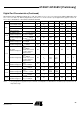
17.14
RX_ACTIVE output
-Saturation voltage high
V
VSINT
= 2.4 V to 5.25 V
I
RX_ACTIVE
= -1.5 mA
46 V
oh
V
AVCC
-
0.5V
V
AVCC
-
0.15V
V B
-Saturation voltage low
V
VSINT
= 2.4 V to 5.25 V
I
RX_ACTIVE
= 25 µA
46 V
ol
0.25 0.4 V B
17.15
DEM_OUT output
Saturation voltage low
Open drain output
I
DEM_OUT
= 250 µA
34 V
ol
0.15 0.4 V B
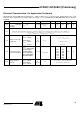
Digital Port Characteristics (Continued)
All parameter refer to GND and valid for T
amb
= -40 °C to +105 °C, V
VS1
= V
S2
= 2.4 V to 3.6 V (1 Battery Application) and
V
VS2
= 4.4 V to 6.6 V (2 Battery Application) and V
VS2
= 4.75 V to 5.25 V (Car Application) typical values at
V
VS1
= V
VS2
= 3V and T
amb
= 25°C unless otherwise specified
No. Parameters Test Conditions Pin Symbol Min. Typ. Max. Unit Type*
*) Type means: A = 100% tested, B = 100% correlation tested, C = Characterized on samples, D = Design parameter
Note: 1. If a logic high level is applied to this pin a minimum serial impedance of 100 Ω must be ensured for proper operation over full
temperature range.