
User guide

83
ATA5811/ATA5812 [Preliminary]
4689B–RKE–04/04
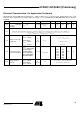
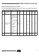
13.5 Baud-rate range
BR_Range =
BR_Range0
BR_Range1
BR_Range2
BR_Range3
BR_Range
1.0
2.0
4.0
8.0
2.5
5.0
10.0
20.0
kBaud A
13.6
Minimum time period
between edges at pin
SDO_TMDO in RX
transparent mode
XLIM = 0
BR_Range_0
BR_Range_1
BR_Range_2
BR_Range_3
XLIM = 1
BR_Range_0
BR_Range_1
BR_Range_2
BR_Range_3
31 T
DATA_min
10 ×
T
XDCLK
µs A
13.7
Edge-to-edge time
period of the data signal
for full sensitivity in RX
mode
BR_Range_0
BR_Range_1
BR_Range_2
BR_Range_3
T
DATA
200
100
50
25
500
250
125
62.5
µs B
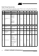
14 TX Mode
14.1 Start-up time From Idle mode T
Startup
331.5
× T
DCLK
331.5
× T
DCLK
µs A
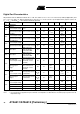
15 Configuration of the Transceiver with 4-wire Serial Interface
15.1
CS set-up time to rising
edge of SCK
33, 35 T
CS_setup
1.5
× T
DCLK
µs A
15.2 SCK cycle time 33 T
Cycle
2 µs A
15.3
SDI_TMDI set-up time
to rising edge of SCK
32, 33 T
Setup
250 ns C
15.4
SDI_TMDI hold time
from rising edge of SCK
32, 33 T
Hold
250 ns C
15.5
SDO_TMDO enable
time from rising edge of
CS
31, 35 T
Out_enable
250 ns C
15.6
SDO_TMDO output
delay from falling edge
of SCK
C
L
= 10 pF 31, 35 T
Out_delay
250 ns C
15.7
SDO_TMDO disable
time from falling edge of
CS
31, 33 T
Out_disable
250 ns C
15.8 CS disable time period 35 T
CS_disable
1.5
× T
DCLK
µs A
Digital Timing Characteristics (Continued)
All parameters refer to GND and are valid for T
amb
= -40°C to +105°C. V
VS1
= V
S2
= 2.4 V to 3.6 V (1-battery application),
V
VS2
= 4.4 V to 6.6 V (2-battery application) and V
VS2
= 4.75 V to 5.25 V (car application), typical values at
V
VS1
= V
VS2
= 3 V and T
amb
= 25°C unless otherwise specified.
No. Parameters Test Conditions Pin Symbol Min. Typ. Max. Unit Type*
*) Type means: A = 100% tested, B = 100% correlation tested, C = Characterized on samples, D = Design parameter