
User guide


74
ATA5811/ATA5812 [Preliminary]
4689B–RKE–04/04
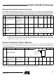
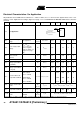
7.4
Current consumption of
the microcontroller
interface
CLK enabled
V
VSOUT
enabled
CLK disabled
V
VSOUT
enabled
V
VSOUT
disabled
C
L
= Load capacitance
on pin CLK
(All interface pins,
except pin CLK, are in
stable condition and
unloaded)
27 I
VSINT
< 10 µA
< 10 µA
7.5
Internal equivalent
capacitance
Used for current
calculation
30, 27 CCLK 8 pF B
8 Power Supply General Definitions and AUX Mode
8.1
Current consumption of
an external device
connected to pin VSOUT
I
EXT
I
EXT
= I
VSOUT
- I
VSINT
I
EXT
= I
VSOUT
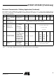
8.2 AUX mode
Electrical Characteristics: General (Continued)
All parameters refer to GND and are valid for T
amb
= -40°C to +105°C, V
VS1
= V
VS2
= 2.4 V to 3.6 V (1-battery application),
V
VS2
= 4.4 V to 6.6 V (2-battery application) and V
VS2
= V
VAUX
= 4.75 V to 5.25 V (car application). Typical values are given
at V
VS1
= V
VS2
= 3 V and T
amb
= 25°C, f
RF
= 433.92 MHz (1-battery application) unless otherwise specified. Details about cur-
rent consumption, timing and digital pin properties can be found in the specific sections of the “Electrical Characteristics”.
No. Parameters Test Conditions Pin
(1)
Symbol Min. Typ. Max. Unit Type*
*) Type means: A = 100% tested, B = 100% correlation tested, C = Characterized on samples, D = Design parameter
Note: 1. Pin numbers in brackets mean they were measured with RF_IN matched to 50 Ω according to Figure 7 on page 10 with
component values according to Table 2 on page 10 and RF_OUT matched to 50 Ω according to Figure 16 on page 19 with
component values according to Table 7 on page 19.
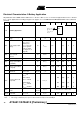
I
VSINT
C
CLK
C
L
+()V
VSINT
f
XTO
××
3
----------------------------------------------------------------------------=
VSINT
VSOUT
I
VSINT
I
VSOUT
I
EXT
VSINT
VSOUT
I
VSINT
I
EXT
= I
VSOUT
VAUX
I
AUX_VAUX