
User guide


73
ATA5811/ATA5812 [Preliminary]
4689B–RKE–04/04
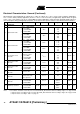
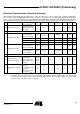
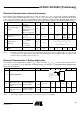
5.10 FSK modulation rate
This correspond to
20 kBaud Manchester
coding and 40 kBaud
NRZ coding
f
Data_FSK
20 kHz B
6 RX/TX Switch
6.1 Impedance RX mode
RX mode, pin 38 with
short connection to
GND, f
RF
= 0 Hz (DC)
39 Z
Switch_RX
23000 Ω A
f
RF
= 315 MHz 39 Z
Switch_RX
(11.3 – j214) Ω C
f
RF
= 433.92 MHz 39 Z
Switch_RX
(10.3 – j153) Ω C
f
RF
= 868.3 MHz 39 Z
Switch_RX
(8.9 – j73) Ω C
6.2 Impedance TX mode
TX mode, pin 38 with
short connection to
GND, f
RF
= 0 Hz (DC)
39 Z
Switch_TX
5 Ω A
f
RF
= 315 MHz
f
RF
= 433.92 MHz
f
RF
= 868.3 MHz
39 Z
Switch_TX
(4.8 + j3.2)
(4.5 + j4.3)
(5 + j9)
Ω
C
C
C
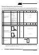
7 Microcontroller Interface
7.1
Voltage range for
microcontroller interface
I
VSINT
< 10 µA if CLK is
disabled and all
interface pins are in
stable condition and
unloaded
27, 28,
29, 30,
31, 32,
33, 34,
35
2.4 5.25 V A
7.2
CLK output rise and fall
time
f
CLK
< 4.5 MHz
C
L
= 10 pF
C
L
= Load capacitance
on pin CLK
2.4 V ≤ V
VSINT
≤ 5.25 V
20% to 80% V
VSINT
30
t
rise
t
fall
20
20
30
30
ns
ns
B
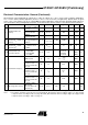
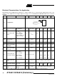
Electrical Characteristics: General (Continued)
All parameters refer to GND and are valid for T
amb
= -40°C to +105°C, V
VS1
= V
VS2
= 2.4 V to 3.6 V (1-battery application),
V
VS2
= 4.4 V to 6.6 V (2-battery application) and V
VS2
= V
VAUX
= 4.75 V to 5.25 V (car application). Typical values are given
at V
VS1
= V
VS2
= 3 V and T
amb
= 25°C, f
RF
= 433.92 MHz (1-battery application) unless otherwise specified. Details about cur-
rent consumption, timing and digital pin properties can be found in the specific sections of the “Electrical Characteristics”.
No. Parameters Test Conditions Pin
(1)
Symbol Min. Typ. Max. Unit Type*
*) Type means: A = 100% tested, B = 100% correlation tested, C = Characterized on samples, D = Design parameter
Note: 1. Pin numbers in brackets mean they were measured with RF_IN matched to 50 Ω according to Figure 7 on page 10 with
component values according to Table 2 on page 10 and RF_OUT matched to 50 Ω according to Figure 16 on page 19 with
component values according to Table 7 on page 19.