
User guide

64
ATA5811/ATA5812 [Preliminary]
4689B–RKE–04/04
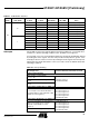
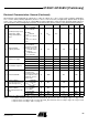
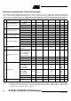
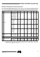
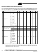
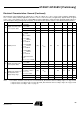
2 Receiver/RX Mode
2.1 Supply current RX mode
f
RF
= 433.92 MHz and
f
RF
= 315 MHz
17, 18 I
S_RX
10.5 mA A
f
RF
= 868 MHz 17, 18 I
S_RX
10.3 mA A
2.2
Supply current
RX polling mode
T
Sleep
= 49.45 ms
X
SLEEP
= 8, Sleep = 5
Baud rate = 20 kBaud
FSK, V
VSOUT
disabled
17, 18 I
P
444 µA B
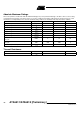
2.3
Input sensitivity FSK
f
RF
= 433.92 MHz
FSK deviation
f
DEV
= ±16 kHz
limits according to
Table 39 on page 57,
BER = 10
-3
T
amb
= 25°C
Baud rate 20 kBaud (4) P
REF_FSK
-104.0 -106.0 -107.5 dBm B
Baud rate 2.4 kBaud (4) P
REF_FSK
-107.5 -109.5 -111.0 dBm B
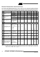
2.4
Input sensitivity ASK
f
RF
= 433.92 MHz
ASK 100%, level of
carrier limits according
to
Table 39 on page 57,
BER = 10
-3
T
amb
= 25°C
Baud rate 10 kBaud (4) P
REF_ASK
-110.5 -112.5 -114.0 dBm B
Baud rate 2.4 kBaud (4) P
REF_ASK
-114.5 -116.5 -118.0 dBm B
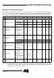
2.5
Sensitivity change at
f
RF
= 315.0 MHz
f
RF
= 868.3 MHz
compared to
f
RF
= 433.92 MHz
f
RF
= 433.92 MHz
to f
RF
= 315.00 MHz
f
RF
= 433.92 MHz to
f
RF
= 868.00 MHz
P = P
REF_ASK
+ ∆P
REF1
+
∆P
REF2
P = P
REF_FSK
+ ∆P
REF1
+
∆P
REF2
(4) ∆P
REF1
-1.0
+2.7
dB B
2.6
Maximum frequency
offset in FSK mode
Maximum frequency
difference of f
RF
between receiver and
transmitter in FSK
mode (f
RF
is the center
frequency of the FSK
signal with
f
DEV
= ±16 kHz)
(4) ∆f
OFFSET
-58 +58 kHz B
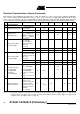
Electrical Characteristics: General (Continued)
All parameters refer to GND and are valid for T
amb
= -40°C to +105°C, V
VS1
= V
VS2
= 2.4 V to 3.6 V (1-battery application),
V
VS2
= 4.4 V to 6.6 V (2-battery application) and V
VS2
= V
VAUX
= 4.75 V to 5.25 V (car application). Typical values are given
at V
VS1
= V
VS2
= 3 V and T
amb
= 25°C, f
RF
= 433.92 MHz (1-battery application) unless otherwise specified. Details about cur-
rent consumption, timing and digital pin properties can be found in the specific sections of the “Electrical Characteristics”.
No. Parameters Test Conditions Pin
(1)
Symbol Min. Typ. Max. Unit Type*
*) Type means: A = 100% tested, B = 100% correlation tested, C = Characterized on samples, D = Design parameter
Note: 1. Pin numbers in brackets mean they were measured with RF_IN matched to 50 Ω according to Figure 7 on page 10 with
component values according to Table 2 on page 10 and RF_OUT matched to 50 Ω according to Figure 16 on page 19 with
component values according to Table 7 on page 19.