
User guide

63
ATA5811/ATA5812 [Preliminary]
4689B–RKE–04/04
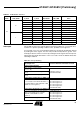
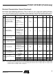
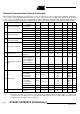
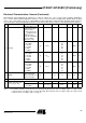
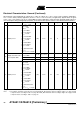
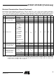
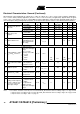
Electrical Characteristics: General
All parameters refer to GND and are valid for T
amb
= -40°C to +105°C, V
VS1
= V
VS2
= 2.4 V to 3.6 V (1-battery application),
V
VS2
= 4.4 V to 6.6 V (2-battery application) and V
VS2
= V
VAUX
= 4.75 V to 5.25 V (car application). Typical values are given
at V
VS1
= V
VS2
= 3 V and T
amb
= 25°C, f
RF
= 433.92 MHz (1-battery application) unless otherwise specified. Details about cur-
rent consumption, timing and digital pin properties can be found in the specific sections of the “Electrical Characteristics”.
No. Parameters Test Conditions Pin
(1)
Symbol Min. Typ. Max. Unit Type*
1 RX_TX_IDLE Mode
1.1
RF operating frequency
range
ATA5811
V
433_N868
= 0 V
4, 10 f
RF
867 870 MHz A
ATA5811
V
433_N868
= AVCC
4, 10 f
RF
433 435 MHz A
ATA5 81 2
V
433_N868
= 0 V
4, 10 f
RF
313 316 MHz A
1.2
Supply current
OFF mode
V
VS1
= V
VS2
= 3 V,
V
VSINT
= 0 V
(1 battery) and
V
VS2
= 6 V (2 battery)
OFF mode is not
available if
V
VS2
= V
VAUX
= 5 V
V
VSINT
= 0 V (car)
I
S_OFF
<10 nA A
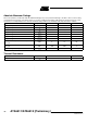
1.3
Supply current
Idle mode
V
VSOUT
disabled,
XTO running
V
VS1
= V
VS2
= 3 V
(1 battery)
I
S_IDLE
220 µA B
V
VS2
= 6 V (2 battery) I
S_IDLE
310 µA B
V
VS2
= V
VAUX
= 5 V (car) I
S_IDLE
310 µA B
1.4 System start-up time
From OFF mode to Idle
mode including reset
and XTO start-up
(see Figure 30 on page
42)
XTAL: C
m
= 5 fF,
C
0
= 1.8 pF, R
m
=15 Ω
T
PWR_ON_IRQ_1
0.3 ms C
1.5 RX start-up time
From Idle mode to
receiving mode
N
Bit-check
= 3
Baud rate = 20 kBaud,
BR_Range_3
(see Figure 40 on page
50 , Figure 41 on page
51 and Figure 42 on
page 52)
T
Startup_PLL
+
T
Startup_Sig_Proc
+ T
Bit-chek
1.39 ms A
1.6 TX start-up time
From Idle mode to TX
mode (see
Figure 50 on
page 59)
T
Startup
0.4 ms A
*) Type means: A = 100% tested, B = 100% correlation tested, C = Characterized on samples, D = Design parameter
Note: 1. Pin numbers in brackets mean they were measured with RF_IN matched to 50 Ω according to Figure 7 on page 10 with
component values according to Table 2 on page 10 and RF_OUT matched to 50 Ω according to Figure 16 on page 19 with
component values according to Table 7 on page 19.