
User guide

36
ATA5811/ATA5812 [Preliminary]
4689B–RKE–04/04
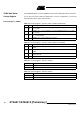
Control Register 3 (ADR 2)
Control Register 4 (ADR 3)
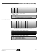
Table 23. Control Register 3 (Function of Bit 3 and Bit 2)
FR8 FR7 Function
00FREQ3 = 0
0 1 FREQ3 = 128
1 0 FREQ3 = 256 (default)
1 1 FREQ3 = 384
Note: Tuning of f
RF
MSB’s
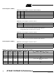
Table 24. Control Register 3 (Function of Bit 1)
VSOUT_EN Function
0 Output voltage power supply for external devices off (pin VSOUT)
1 Output voltage power supply for external devices on (default)
Note: This bit is set to 1 if the Bit-check is ok (RX_Polling, RX mode), an event at pin T1, T2,
T3, T4 or T5 occurs or the bit Power_On in the status register is 1.
Setting VSOUT_EN = 0 in AUX mode is not allowed
Table 25. Control Register 3 (Function of Bit 0)
CLK_ON Function
0 Clock output off (pin CLK)
1 Clock output on (default)
Note: This bit is set to 1 if the Bit-check is ok (RX_Polling, RX mode), an event at pin T1, T2,
T3, T4 or T5 occurs or the bit Power_On in the status register is 1.
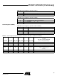
Table 26. Control Register 4 (Function of Bit 7)
ASK_NFSK Function
0 FSK mode (default)
1 ASK mode
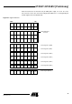
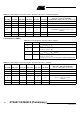
Table 27. Control Register 4 (Function of Bit 6, Bit 5, Bit 4, Bit 3 and Bit 2)
Sleep4 Sleep3 Sleep2 Sleep1 Sleep0
Function Sleep
(T
Sleep
= Sleep × 1024 × T
DCLK
× X
Sleep
)
00000 0
00001 1
.....
01010
10
(T
Sleep
= 10 × 1024 × T
DCLK
× X
Sleep
)
(default)
.....
11111 31