
User guide

35
ATA5811/ATA5812 [Preliminary]
4689B–RKE–04/04
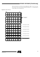
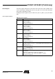
Control Register 2 (ADR 1)
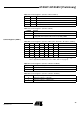
Table 18. Control Register 1 (Function of Bit 2 and Bit 1)
OPM1 OPM0 Function
0 0 Idle mode (default)
01TX mode
1 0 RX polling mode
11RX mode
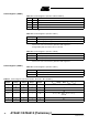
Table 19. Control Register 1 (Function of Bit 0)
T_MODE Function
0 TX and RX function via TX/RX data buffer (default)
1
Transparent mode, TX/RX data buffer disabled, TX modulation data stream via
pin SDI_TMDI, RX modulation data stream via pin SDO_TMDO
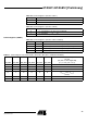
Table 20. Control Register 2 (Function of Bit 7, Bit 6, Bit 5, Bit 4, Bit 3, Bit 2 and Bit 1)
FR6 FR5 FR4 FR3 FR2 FR1 FR0 Function
0000000FREQ2 = 0
0000001FREQ2 = 1
.......
1011000FREQ2 = 88 (default)
.......
1111111FREQ2 = 127
Note: Tuning of f
RF
LSB’s (total 9 bits), frequency trimming, resolution of f
RF
is f
XTO
/16384
which is approximately 800 Hz (see section “XTO”, Table 12 on page 24)
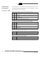
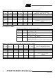
Table 21. Control Register 2 (Function of Bit 0 in RX Mode)
P_MODE Function (RX Mode)
0 Pin IRQ is set to 1 if the Bit-check is successful (default)
1 No effect on pin IRQ if the Bit-check is successful
Table 22. Control Register 2 (Function of Bit 0 in TX Mode)
P_MODE Function (TX Mode)
0 Manchester modulator on (default)
1 Manchester modulator off (NRZ mode)