
User guide

32
ATA5811/ATA5812 [Preliminary]
4689B–RKE–04/04
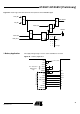
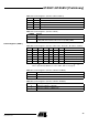
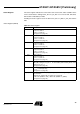
2-Battery Application The supply voltage range is 4.4 V to 6.6 V and VAUX is connected to an inductive
supply.
Figure 26. 2-Battery Application with Inductive Emergency Supply
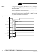
Microcontroller
Interface
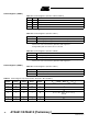
The microcontroller interface is a level converter which converts all internal digital sig-
nals which are referred to the DVCC voltage, into the voltage used by the
microcontroller. Therefore, the pin VSINT has to be connected to the supply voltage of
the microcontroller.
This makes it possible to use the internal voltage regulator/switch at pin VSOUT as in
Figure 4 on page 6 and Figure 6 on page 8 or to connect the microcontroller and the pin
VSINT directly to the supply voltage of the microcontroller as in Figure 5 on page 7.
Digital Control Logic
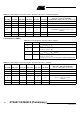
Register Structure The configuration of the transceiver is stored in RAM cells. The RAM contains a
16 × 8-bit TX/RX data buffer and a 6 × 8-bit control register and is write and readable
via a 4-wire serial interface (CS, SCK, SDI_TMDI, SDO_TMDO).
The 1 × 8-bit status register is not part of the RAM and is readable via the 4-wire serial
interface.
The RAM and the status information is stored as long as the transceiver is in any active
mode (DVCC = VS1 or DVCC = V_REG2) and gets lost if the transceiver is in OFF
mode (DVCC = OFF).
VS1
VS2
VAUX
Microcontroller
ATA5811/ATA5812
4.4 V to 6.6 V
VSOUT
VSINT
VS
AVCC
DVCC
CS
SCK
SDI_TMDI
SDO_TMDO
IRQ
CLK
NRESET
OUT
OUT
OUT
IN
IN
IN
IN
Microcontoller_Interface
DEM_OUT
RF - Transceiver
Digital Control
Logic