
User guide

3
ATA5811/ATA5812 [Preliminary]
4689B–RKE–04/04
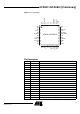
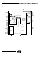
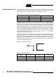
Figure 2. Pinning QFN48
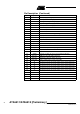
Pin Description
Pin Symbol Function
1 NC Not connected
2 NC Not connected
3 NC Not connected
4RF_INRF input
5 NC Not connected
6 433_N868 Selects RF input/output frequency range
7 NC Not connected
8 R_PWR Resistor to adjust output power
9 PWR_H Pin to select output power
10 RF_OUT RF output
11 NC Not connected
12 NC Not connected
13 NC Not connected
14 NC Not connected
15 NC Not connected
16 AVCC Blocking of the analog voltage supply
17 VS2 Power supply input for voltage range 4.4 V to 6.6 V
18 VS1 Power supply input for voltage range 2.4 V to 3.6 V
NC
NC
NC
RF_IN
NC
433_N868
NC
R_PWR
PWR_H
RF_OUT
NC
NC
RSSI
CS
DEM_OUT
SCK
SDI_TMDI
SDO_TMDO
CLK
IRQ
N_RESET
VSINT
NC
XTAL2
NC
NC
RX_ACTIVE
T1
T2
T3
T4
T5
PWR_ON
RX_TX1
RX_TX2
CDEM
NC
NC
NC
AVCC
VS2
VS1
VAUX
TEST1
DVCC
VSOUT
TEST2
XTAL1
48 47 46 45 44 43 42 41 40 39 38 37
13 14 15 16 17 18 19 20 21 22 23 24
1
2
3
4
5
6
7
8
9
10
11
12
36
35
34
33
32
31
30
29
28
27
26
25
ATA5811/ATA5812