
User guide


24
ATA5811/ATA5812 [Preliminary]
4689B–RKE–04/04
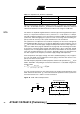
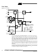
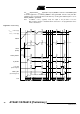
Figure 19. XTO Block Diagram
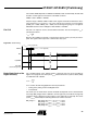
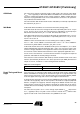
To find the right values used in the control registers 2 and 3 (see Table 20 on page 35
and Table 23 on page 36) the relationship between f
XTO
and the f
RF
is shown in
Table 12. To determine the right content the frequency at pin CLK as well as the output
frequency at RF_OUT in ASK mode can be measured, than the FREQ value can be cal-
culated according to Table 12 so that f
RF
is exactly the desired radio frequency
S1 S2
XTAL1 XTAL2
C
L1
C
L2
10 pF 10 pF
Divider
/3
CLK
CLK_ON
(Control
Register 3)
Divider
/16
f
DCLK
f
XTO
Divider
/1
/2
/4
/8
/16
f
XDCLK
Baud1
Baud0
XLim
8 pF 8 pF
In IDLE mode and during Sleep mode (RX_Polling) the
switches S1 and S2 are open.
Amplitude
Detector
XTO_OK
(to Reset Logic)
VSOUT_OK
(from power supply)
&
DVCC_OK
(from power supply)
Table 12. Calculation of f
RF
Frequency (MHz)
Pin 6
433_N868
CREG1
Bit(4)
FS f
XTO
(MHz) f
RF
= f
TX_ASK
= f
RX
f
TX_FSK_L
f
TX_FSK_H
433.92 AVCC 0 13.25311 f
RF
- 16.17 kHz f
RF
+ 16.17 kHz
868.3 GND 0 13.41191 f
RF
- 16.37 kHz f
RF
+ 16.37 kHz
315.0 AVCC 1 12.73193 f
RF
- 15.54 kHz f
RF
+ 15.54 kHz
f
XTO
32 5
FREQ 20,5+
16384
----------------------------------+,
⎝⎠
⎛⎞
×
f
XTO
64 5
FREQ 20,5+
16384
----------------------------------+,
⎝⎠
⎛⎞
×
f
XTO
24 5
FREQ 20,5+
16384
----------------------------------+,
⎝⎠
⎛⎞
×