
User Manual


3
ATA5756/ATA5757 [Preliminary]
4702D–RKE–02/04
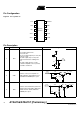
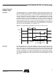
4 ANT2 Emitter of antenna output stage
5 ANT1 Open collector antenna output
6 XTO2 Diode switch, used for FSK modulation
7 XTO1 Connection for crystal
8 VS Supply voltage See ESD protection circuitry (see Figure 12)
9 GND Ground See ESD protection circuitry (see Figure 12)
10 ENABLE
ENABLE input
If ENABLE is connected to GND and
the ASK or FSK pin is High, the device
stays in idle mode.
In normal operation ENABLE is left
open and ASK or FSK is used to enable
the device.
Pin Description
Pin Symbol Function Configuration
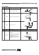
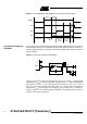
ANT1
ANT2
XTO2
210 µA
(FSK < 0.25V)
AND
(ENABLE > 1.7V)
XTO1
1.2k
VS
1.5k
VS
182 µA
ENABLE
150k
30 µA
(FSK >1.7 V ) OR
(ASK > 1.7 V)
250k
VS