
User Manual

16
ATA5756/ATA5757 [Preliminary]
4702D–RKE–02/04
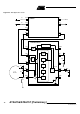
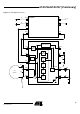
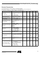
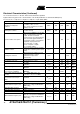
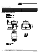
Imaginary part of XTO1
Impedance in stady state
oscillation
Since pulling P is
P = -IM
XTO
× C
M
× π × f
XTO
∆f
XTO
can be calculated out of IM
XTO
with C
M
=4.37fF
IM
XTO
j20 j110 j200 Ω
Real part of XTO1 impedance in
small signal oscillation
This value is important for crystal
oscillator start-up
RE
XTO
-650 -1100 Ω
Crystal oscillator start-up time
Time between ENABLE of the IC with
FSK = H and activation of the CLK
output. The CLK is activated
synchronously to the output frequency
if the current through the XTAL has
reached 35% to 80% of its maximum
amplitude. Crystal parameters:
C
M
= 4.37 fF, C
0
= 1.3 pF,
C
LNOM
= 18 pF, C
4
= 10 pF,
C
5
= 15 pF, R
S
≤60 Ω
∆T
XTO
0.6 1.4 ms
XTO drive current
Current flowing through the crystal in
steady state oscillation (peak-to-peak
value)
I
DXTO
300 µApp
Locking time of the PLL
Time between the activation of CLK
and when the PLL is locked
(transmitter ready for data
transmission)
∆Τ
PLL
250 µs
PLL loop bandwidth f
Loop_PLL
250 kHz
In loop phase noise PLL 25 kHz distance to carrier L
PLL
-85 -76 dBc/Hz
Phase noise VCO
at 1 MHz
at 36 MHz
L
at1M
L
at36M
-90
-121
-84
-115
dBc/Hz
dBc/Hz
Frequency range of VCO
ATA5756
ATA5757
f
VCO
310
432
317
448
MHz
MHz
Clock output frequency (CMOS
microcontroller compatible)
ATA5756
ATA5757
f
CLK
f
0
/192
f
0
/256
MHz
Clock output minimum High and
Low time
C
Load
≤ 20 pF, High = 0.8 × Vs,
Low = 0.2 × V
S
, f
CLK
<1.7MHz
T
CLKLH
125 ns
Series resonance resistance of
the resonator seen from pin
XTO1
For proper detection of the XTO
amplitude
R
s_max
150 Ω
Capacitive load at Pin XTO1 C
L_max
5 pF
FSK modulation frequency rate
This corresponds to 20 kBaud in
Manchester coding and 40 kBaud in
NRZ coding
f
MOD_FSK
0 20 kHz
FSK switch OFF resistance High Z R
SWIT_OFF
50 kΩ
FSK switch OFF capacitance High Z capacitance C
SWIT_OFF
0.75 0.9 1.1 pF
FSK switch ON resistance Low Z R
SWIT_ON
130 175 Ω
ASK modulation frequency rate
Duty cycle of the modulation signal =
50%, this corresponds to 20 kBaud in
Manchester coding and 40 kBaud in
NRZ coding
f
MOD_ASK
0 20 kHz
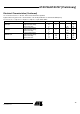
Electrical Characteristics (Continued)
V
S
= 2.0 V to 3.6 V, T
amb
= -40°C to 125°C unless otherwise specified.
Typical values are given at V
S
= 3.0 V and T
amb
= 25°C. All parameters are referred to GND (Pin 9).
C
M
= 4.37 fF, C
0
= 1.3 pF, C
LNOM
= 18 pF, C
4
= 10 pF, C
5
= 15 pF and R
S
≤60 Ω
Parameters Test Conditions Symbol Min. Typ. Max. Unit