
User Manual

15
ATA5756/ATA5757 [Preliminary]
4702D–RKE–02/04
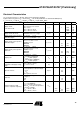
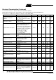
Electrical Characteristics
V
S
= 2.0 V to 3.6 V, T
amb
= -40°C to 125°C unless otherwise specified.
Typical values are given at V
S
= 3.0 V and T
amb
= 25°C. All parameters are referred to GND (Pin 9).
C
M
= 4.37 fF, C
0
= 1.3 pF, C
LNOM
= 18 pF, C
4
= 10 pF, C
5
= 15 pF and R
S
≤60 Ω
Parameters Test Conditions Symbol Min. Typ. Max. Unit
Supply current,
power-down mode
V
ENABLE
< 0.25 V or ENABLE is open,
V
ASK
<0.25V, V
FSK
<0.25V
T
amb
=25°C
T
amb
=-40°C to +85°C
T
amb
=-40°C to +125°C
I
S_Off
1 100
350
7,000
nA
nA
nA
Supply current, idle mode
V
ENABLE
< 0.25 V, V
S
≤3.2 V
ASK,FSK can be Low or High
I
S_IDLE
100 µA
Supply current, power-up, PA off,
FSK switch High Z
V
S
≤3.2 V, V
FSK
>1.7V,
V
ASK
< 0.25 V ENABLE is open
I
S
3.6 4.6 mA
Supply current, power-up, PA on,
FSK switch High Z
V
S
≤ 3.2 V, C
CLK
≤ 10 pF
V
FSK
> 1.7 V, V
ASK
>1.7V
ENABLE is open
ATA5756
ATA5757
I
S_Transmit1
8.1
8.5
9.8
10.5
mA
mA
Supply current, power-up, PA on,
FSK Low Z
V
S
≤ 3.2 V, C
CLK
≤ 10 pF
V
FSK
<0.25V, V
ASK
>1.7V
ENABLE is open
ATA5756
ATA5757
I
S_Transmit2
8.4
8.8
10.2
11.0
mA
mA
Output power
V
S
= 3.0 V, T
amb
=25° C,
f = 315 MHz for
ATA57 56 ,
Z
Load, opt
= (380 + j340) Ω
f = 433.92 MHz for
ATA5757,
Z
Load, opt
= (280 + j310) Ω
P
Out
4 6 8 dBm
Output power variation for the full
temperature and supply voltage
range
T
amb
= -40°C to +125°C,
V
S
= 2.0 V to 3.2 V
P
Out
1 8 dBm
Spurious emission
f
CLK
= f
XT0
/8
Load capacitance at pin CLK ≤ 20 pF
f
0
±f
CLK
f
0
±f
XT0
other spurious are lower
Spour -42
-60
dBc
Harmonics
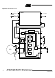
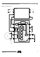
With 50 Ω matching network according
to Figure 9
2nd
3rd
-16
-15
dBc
dBc
Oscillator frequency XTO
(= phase comparator frequency)
f
XTO
= f
0
/24 ATA5756
f
XTO
= f
0
/32 ATA5757
f
XTAL
= resonant frequency of the
XTAL, C
M
= 4.37 fF, load capacitance
selected accordingly
T
amb
= -40°C to +85°C
T
amb
= -40°C to +125°C
∆f
XTO
-14.0
-17.5
f
XTAL
f
XTAL
+14.0
+17.5
ppm
ppm