
Owner manual

AT90C8534
45
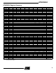
Electrical Characteristics
Notes: 1. “Max” means the highest value where the pin is guaranteed to be read as low (logical “0”).
2. “Min” means the lowest value where the pin is guaranteed to be read as high (logical “1”).
3. Although each I/O port can sink more than the test conditions (1 mA at V
CC
= 2.2V) under steady-state conditions
(non-transient), the following must be observed:
The sum of all I
OL
, for all ports, should not exceed 80 mA.
If I
OL
exceeds the test condition, V
OL
may exceed the related specification. Pins are not guaranteed to sink current greater
than the listed test condition.
4. Although each I/O port can source more than the test conditions (1 mA at V
CC
= 2.2V) under steady-state conditions (non--
transient), the following must be observed:
The sum of all I
OH
, for all ports, should not exceed 80 mA.
If I
OH
exceeds the test condition, V
OH
may exceed the related specification. Pins are not guaranteed to source current
greater than the listed test condition.
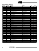
Absolute Maximum Ratings*
Operating Temperature ................................. -40°C to +105°C
*NOTICE: Stresses beyond those listed under “Absolute
Maximum Ratings” may cause permanent dam-
age to the device. This is a stress rating only and
functional operation of the device at these or
other conditions beyond those indicated in the
operational sections of this specification is not
implied. Exposure to absolute maximum rating
conditions for extended periods may affect device
reliability.
Storage Temperature .................................... -65°C to +150°C
Voltage on any Pin
with respect to Ground ..............................-1.0V to V
CC
+ 0.5V
Maximum Operating Voltage ............................................ 6.6V
I/O Pin Maximum Current ........................................... 20.0 mA
Maximum Current VCC and GND............................. 100.0 mA
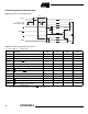
DC Characteristics
T
A
= -40°C to 85°C, V
CC
= 3.3V to 6.0V (unless otherwise noted)
Symbol Parameter Condition Min Typ Max Units
V
IL
Input Low Voltage -0.5 0.3 V
CC
(1)
V
V
IL1
Input Low Voltage XTAL -0.5 0.2 V
CC
(1)
V
V
IH
Input High Voltage Except XTAL, RESET 0.6 V
CC
(2)
V
CC
+ 0.5 V
V
IH1
Input High Voltage XTAL 0.8 V
CC
(2)
V
CC
+ 0.5 V
V
IH2
Input High Voltage RESET 0.9 V
CC
(2)
V
CC
+ 0.5 V
V
OL
Output Low Voltage
(3)
(Port A) I
OL
= 1 mA, V
CC
= 2.5V 0.1 V
V
OH
Output High Voltage
(4)
(Port A) I
OH
= -1 mA, V
CC
= 2.5V 1.44 V
I
IL
Input Leakage Current (I/O pin) V
CC
= 6V, pin low -8.0 µA
I
IH
Input Leakage Current (I/O pin) V
CC
= 6V, pin high 8.0 µA
RRST Reset Pull-up 100 500 K
Ω
RPEN PEN Pull-up 30 250 KΩ
I
CC
Power Supply Current
Active 1 MHz, V
CC
= 3.6V,
ADC disabled
1.5 2.0 mA
Active 1 MHz, V
CC
= 3.6V,
ADC enabled
1.9 2.7 mA
Idle 1 MHz, V
CC
= 3.6V,
ADC disabled
0.25 1.0 mA
Idle 1 MHz, V
CC
= 3.6V,
ADC enabled
0.7 1.7 mA
Power-down, V
CC
= 3.6V 1 10 µA