
Owner manual


AT90C8534
39
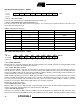
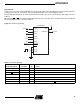
Signal Names
In this section, some pins of the AT90C8534 are referenced by signal names describing their function during parallel pro-
gramming. See Figure 35 and Table 11. Pins not described in Table 11 are referenced by pin names.
The XA1/XA0 pins determines the action executed when the XTAL1 pin is given a positive pulse. The coding is shown in
Table 12.
When pulsing WR
or OE, the command loaded determines the action executed. The command is a byte where the different
bits are assigned functions as shown in Table 13.
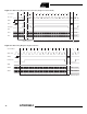
Figure 35. Parallel Programming
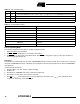
Table 11. Pin Name Mapping
Signal Name in
Programming Mode Pin Name I/O Function
RDY/BSY
INT1 O “0”: Device is busy programming, “1”: Device is ready for new command
OE ADIN1 I Output Enable (active low)
WR
ADIN2 I Write Pulse (active low)
BS ADIN3 I Byte Select (“0” selects low byte, “1” selects high byte)
XA0 ADIN4 I XTAL1 Action Bit 0
XA1 ADIN5 I XTAL1 Action Bit 1
DATA INT0, PA6-0 I/O Bi-directional Data Bus (output when OE
is low)
AT90VC8534
VCC
+5V
RESET
GND
XTAL1
RESET
RDY/BSY
OE
BS
XA0
XA1
WR
DATA
PEN
INT1
ADIN1
ADIN2
ADIN3
ADIN4
ADIN5
INT0,PA6-0