
Owner manual


AT90C8534
37
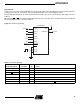
Note: 1. AV
CC
must not go below 3.3V or above 6.0V.
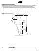
Output Port A
Port A is a 7-bit general output port with tri-state mode.
The port has true read-modify-write functionality. This means that one port pin can be tri-stated without unintentionally
tri-stating any other pin with the SBI and CBI instructions. The same applies for changing drive value.
Two I/O memory address locations are allocated for Port A, one each for the Data Register – PORTA, $1B($3B) and Data
Direction Register – DDRA, $1A($3A). Both locations are read/write.
The Port A output buffers can sink 20 mA and thus drive LED displays directly.
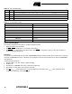
Port A Data Register – PORTA
Port A Data Direction Register – DDRA
All seven pins in Port A have equal functionality.
PAn, General Output pin: The DDAn bit in the DDRA register selects tri-state mode of this pin. If DDAn is set (one), PAn is
configured to drive out the value in PORTAn. If DDAn is cleared (zero), PAn is configured as a tri-state pin.
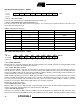
ADC Characteristics
T
A
= -40°C to 85°C
Symbol Parameter Condition Min Typ Max Units
Resolution 10 Bits
Absolute Accuracy AV
CC
= 3.3 - 6.0V 2 LSB
INL Integral Nonlinearity AV
CC
= 3.3 - 6.0V 1 LSB
DNL Differential Nonlinearity AV
CC
= 3.3 - 6.0V 2 LSB
Zero Error (Offset) AV
CC
= 3.3 - 6.0V 0.5 LSB
Conversion Time 76 175 µs
Clock Frequency 80 170 kHz
AV
CC
Analog Supply Voltage V
CC
- 0.3
(1)
V
CC
+ 0.3
(1)
V
R
REF
Reference Input Resistance 6 10 13 KΩ
R
AIN
Analog Input Resistance 100 MΩ
Bit 76543210
$1B ($3B) – PORTA6 PORTA5 PORTA4 PORTA3 PORTA2 PORTA1 PORTA0 PORTA
Read/Write R R/W R/W R/W R/W R/W R/W R/W
Initial value 0 0 0 0 0 0 0 0
Bit 76543210
$1A ($3A) – DDA6 DDA5 DDA4 DDA3 DDA2 DDA1 DDA0 DDRA
Read/Write R R/W R/W R/W R/W R/W R/W R/W
Initial value 0 0 0 0 0 0 0 0