
User guide

23
AT89C55WD
1921B–MICRO–09/02
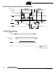
Programming
Interface
Every code byte in the Flash array can be programmed by using the appropriate combination
of control signals. The write operation cycle is self-timed and once initiated, will automatically
time itself to completion.
Most worldwide major programming vendors offer support for the Atmel microcontroller series.
Please contact your local programming vendor for the appropriate software revision.
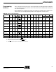
Notes: 1. Write Code Data requires a 200 ns PROG pulse.
2. Write Lock Bits requires a 100 µs PROG
pulse.
3. Chip Erase requires a 200 ns - 500 ns PROG
pulse.
4. RDY/BSY
signal is output on P3.0 during programming.
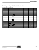
Table 1 0. Flash Programming Modes
Mode V
CC
RST PSEN
ALE/
PROG
EA/
V
PP
P2.6 P2.7 P3.3 P3.6 P3.7
P0.7-0
Data
P3.4 P2.5-0 P1.7-0
Address
WriteCodeData 5V H L
(1)
12V L H H H H D
IN
A14 A13-8 A7-0
Read Code Data 5V H L H H/12V L L L H H D
OUT
A14 A13-8 A7-0
Write Lock Bit 1 6.5V H L
(2)
12V H H H H H X X X X
Write Lock Bit 2 6.5V H L
(2)
12V H H H L L X X X X
Write Lock Bit 3 6.5V H L
(2)
12V H L H H L X X X X
Read Lock Bits
1, 2, 3
5V H L H H H H L H L
P0.2,
P0.3,
P0.4
XX X
Chip Erase 6.5V H L
(3)
12V H L H L L X X X X
Read Atmel ID 5V H L H H L L L L L 1EH X XX 0000 00H
Read Device ID 5V H L H H L L L L L 55H X XX 0001 00H
Read Device ID 5V H L H H L L L L L 06H X XX 0010 00H