Features • • • • • • • • • • • • • • • • Compatible with MCS®-51 Products 20K Bytes of Reprogrammable Flash Memory Endurance: 1000 Write/Erase Cycles 4V to 5.
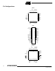
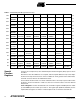
Pin Configurations 44 43 42 41 40 39 38 37 36 35 34 P1.4 P1.3 P1.2 P1.1 (T2 EX) P1.0 (T2) NC VCC P0.0 (AD0) P0.1 (AD1) P0.2 (AD2) P0.3 (AD3) TQFP 33 32 31 30 29 28 27 26 25 24 23 1 2 3 4 5 6 7 8 9 10 11 P0.4 (AD4) P0.5 (AD5) P0.6 (AD6) P0.7 (AD7) EA/VPP NC ALE/PROG PSEN P2.7 (A15) P2.6 (A14) P2.5 (A13) (WR) P3.6 (RD) P3.7 XTAL2 XTAL1 GND GND (A8) P2.0 (A9) P2.1 (A10) P2.2 (A11) P2.3 (A12) P2.4 12 13 14 15 16 17 18 19 20 21 22 P1.5 P1.6 P1.7 RST (RXD) P3.0 NC (TXD) P3.1 (INT0) P3.2 (INT1) P3.
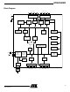
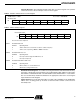
AT89C55WD Block Diagram P0.0 - P0.7 P2.0 - P2.7 PORT 0 DRIVERS PORT 2 DRIVERS VCC GND RAM ADDR. REGISTER B REGISTER PORT 0 LATCH RAM QUICK FLASH PORT 2 LATCH STACK POINTER ACC BUFFER TMP1 TMP2 PROGRAM ADDRESS REGISTER PC INCREMENTER ALU INTERRUPT, SERIAL PORT, AND TIMER BLOCKS PROGRAM COUNTER PSW PSEN ALE/PROG EA / VPP TIMING AND CONTROL DUAL DPTR INSTRUCTION REGISTER RST WATCH DOG PORT 1 LATCH PORT 3 LATCH PORT 1 DRIVERS PORT 3 DRIVERS OSC P1.0 - P1.7 P3.0 - P3.
Pin Description VCC Supply voltage. GND Ground. Port 0 Port 0 is an 8-bit open drain bi-directional I/O port. As an output port, each pin can sink eight TTL inputs. When 1s are written to port 0 pins, the pins can be used as high-impedance inputs. Port 0 can also be configured to be the multiplexed low-order address/data bus during accesses to external program and data memory. In this mode, P0 has internal pull-ups.
AT89C55WD Port Pin Alternate Functions P3.0 RXD (serial input port) P3.1 TXD (serial output port) P3.2 INT0 (external interrupt 0) P3.3 INT1 (external interrupt 1) P3.4 T0 (timer 0 external input) P3.5 T1 (timer 1 external input) P3.6 WR (external data memory write strobe) P3.7 RD (external data memory read strobe) RST Reset input. A high on this pin for two machine cycles while the oscillator is running resets the device.
Table 1.
AT89C55WD Interrupt Registers: The individual interrupt enable bits are in the IE register. Two priorities can be set for each of the six interrupt sources in the IP register. Table 2. T2CON—Timer/Counter 2 Control Register T2CON Address = 0C8H Reset Value = 0000 0000B Bit Addressable Bit TF2 EXF2 RCLK TCLK EXEN2 TR2 C/T2 CP/RL2 7 6 5 4 3 2 1 0 Table 3.
Table 4.
AT89C55WD Memory Organization MCS-51 devices have a separate address space for Program and Data Memory. Up to 64 Kbytes each of external Program and Data Memory can be addressed. Program Memory If the EA pin is connected to GND, all program fetches are directed to external memory. On the AT89C55WD, if EA is connected to VCC, program fetches to addresses 0000H through 4FFFH are directed to internal memory and fetches to addresses 5000H through FFFFH are to external memory.
Hardware Watchdog Timer (One-time Enabled with Reset-out) The WDT is intended as a recovery method in situations where the CPU may be subjected to software upsets. The WDT consists of a 13-bit counter and the WatchDog Timer Reset (WDTRST) SFR. The WDT is defaulted to disable from exiting reset. To enable the WDT, a user must write 01EH and 0E1H in sequence to the WDTRST register (SFR location 0A6H). When the WDT is enabled, it will increment every machine cycle while the oscillator is running.
AT89C55WD Timer 0 and 1 Timer 0 and Timer 1 in the AT89C55WD operate the same way as Timer 0 and Timer 1 in the AT89C51 and AT89C52. Timer 2 Timer 2 is a 16-bit Timer/Counter that can operate as either a timer or an event counter. The type of operation is selected by bit C/T2 in the SFR T2CON (shown in Table 2). Timer 2 has three operating modes: capture, auto-reload (up or down counting), and baud rate generator. The modes are selected by bits in T2CON, as shown in Table 2.
Figure 5. Timer in Capture Mode ÷12 OSC C/T2 = 0 TH2 TL2 OVERFLOW CONTROL C/T2 = 1 TF2 TR2 CAPTURE T2 PIN RCAP2H RCAP2L TRANSITION DETECTOR TIMER 2 INTERRUPT T2EX PIN EXF2 CONTROL EXEN2 Figure 6 shows Timer 2 automatically counting up when DCEN=0. In this mode, two options are selected by bit EXEN2 in T2CON. If EXEN2 = 0, Timer 2 counts up to 0FFFFH and then sets the TF2 bit upon overflow. The overflow also causes the timer registers to be reloaded with the 16-bit value in RCAP2H and RCAP2L.
AT89C55WD Figure 6. Timer 2 Auto Reload Mode (DCEN = 0) ÷12 OSC C/T2 = 0 TH2 TL2 OVERFLOW CONTR OL TR2 C/T2 = 1 RELO AD T2 PIN RCAP2H TIMER 2 INTERRUPT RCAP2L TF2 TRANSITION DETECTOR EXF2 T2EX PIN CONTROL EXEN2 Table 6.
Figure 7. Timer 2 Auto Reload Mode (DCEN = 1) TOGGLE (DOWN COUNTING RELOAD VALUE) 0FFH 0FFH ÷ 12 OSC EXF2 OVERFLOW C/T2 = 0 TH2 TL2 TF2 CONTROL TR2 TIMER 2 INTERRUPT C/T2 = 1 T2 PIN RCAP2H RCAP2L COUNT DIRECTION 1=UP 0=DO (UP COUNTING RELOAD VALUE) T2EX PIN Figure 8. Timer 2 in Baud Rate Generator Mode TIMER 1 OVERFLOW ÷2 "0" "1" NOTE: OSC. FREQ.
AT89C55WD Baud Rate Generator Timer 2 is selected as the baud rate generator by setting TCLK and/or RCLK in T2CON (Table 2). Note that the baud rates for transmit and receive can be different if Timer 2 is used for the receiver or transmitter and Timer 1 is used for the other function. Setting RCLK and/or TCLK puts Timer 2 into its baud rate generator mode, as shown in Figure 8.
Figure 9. Timer 2 in Clock-Out Mode TL2 (8-BITS) 2 OSC TH2 (8-BITS) TR2 RCAP2L RCAP2H C/T2 BIT P1.0 (T2) 2 T2OE (T2MOD.1) TRANSITION DETECTOR P1.
AT89C55WD Programmable Clock Out A 50% duty cycle clock can be programmed to come out on P1.0, as shown in Figure 9. This pin, besides being a regular I/O pin, has two alternate functions. It can be programmed to input the external clock for Timer/Counter 2 or to output a 50% duty cycle clock ranging from 61 Hz to 4 MHz for a 16 MHz operating frequency. To configure the Timer/Counter 2 as a clock generator, bit C/T2 (T2CON.1) must be cleared and bit T2OE (T2MOD.1) must be set. Bit TR2 (T2CON.
Table 7. Interrupt Enable (IE) Register (MSB) EA (LSB) – ET2 ES ET1 EX1 ET0 EX0 Enable Bit = 1 enables the interrupt. Enable Bit = 0 disables the interrupt. Symbol Position Function EA IE.7 Disables all interrupts. If EA = 0, no interrupt is acknowledged. If EA = 1, each interrupt source is individually enabled or disabled by setting or clearing its enable bit. – IE.6 Reserved. ET2 IE.5 Timer 2 interrupt enable bit. ES IE.4 Serial Port interrupt enable bit. ET1 IE.
AT89C55WD Oscillator Characteristics XTAL1 and XTAL2 are the input and output, respectively, of an inverting amplifier that can be configured for use as an on-chip oscillator, as shown in Figure 11. Either a quartz crystal or ceramic resonator may be used. To drive the device from an external clock source, XTAL2 should be left unconnected while XTAL1 is driven, as shown in Figure 12.
Figure 12. External Clock Drive Configuration NC XTAL2 EXTERNAL OSCILLATOR SIGNAL XTAL1 GND Table 8.
AT89C55WD Program Memory Lock Bits The AT89C55WD has three lock bits that can be left unprogrammed (U) or can be programmed (P) to obtain the additional features listed in the following table. Table 9. Lock Bit Protection Modes Program Lock Bits 1 LB1 LB2 LB3 Protection Type U U U No program lock features.
puts, and the next cycle may begin. Data Polling may begin any time after a write cycle has been initiated. Ready/Busy: The progress of byte programming can also be monitored by the RDY/BSY output signal. P3.0 is pulled low after ALE goes high during programming to indicate BUSY. P3.0 is pulled high again when programming is done to indicate READY. Program Verify: If lock bits LB1 and LB2 have not been programmed, the programmed code data can be read back via the address and data lines for verification.
AT89C55WD Programming Interface Every code byte in the Flash array can be programmed by using the appropriate combination of control signals. The write operation cycle is self-timed and once initiated, will automatically time itself to completion. Most worldwide major programming vendors offer support for the Atmel microcontroller series. Please contact your local programming vendor for the appropriate software revision. Table 10. Flash Programming Modes Mode VCC RST PSEN ALE/ PROG P3.4 P2.5-0 P1.
Figure 13. Programming the Flash Memory 4.5V to 5.5V AT89C55WD ADDR. 0000H/4FFFH A0 - A7 A8 - A13 A14* SEE FLASH PROGRAMMING MODES TABLE P1.0 - P1.7 VCC P2.0 - P2.5 P3.4 P2.6 P2.7 P3.3 P3.6 P0 PGM DATA ALE PROG EA VIH /VPP P3.7 XTAL2 3 - 33 MHz XTAL1 GND P3.0 RDY/ BSY RST VIH PSEN Figure 14. Verifying the Flash Memory 4.5V to 5.5V AT89C55WD A0 - A7 ADDR. 0000H/4FFFH P1.0 - P1.7 VCC P2.0 - P2.5 P3.4 P2.6 P2.7 P3.3 P3.6 P3.
AT89C55WD Flash Programming and Verification Characteristics TA = 20°C to 30°C, VCC = 4.5V to 5.5V Symbol Parameter Min Max Units VPP Programming Supply Voltage 11.5 12.5 V IPP Programming Supply Current 10 mA ICC VCC Supply Current 30 mA 1/tCLCL Oscillator Frequency 33 MHz tAVGL Address Setup to PROG Low 48tCLCL tGHAX Address Hold After PROG 48tCLCL tDVGL Data Setup to PROG Low 48tCLCL tGHDX Data Hold After PROG 48tCLCL tEHSH P2.
Flash Programming and Verification Waveforms PROGRAMMING ADDRESS P1.0 - P1.7 P2.0 - P2.5 P3.4 VERIFICATION ADDRESS tAVQV PORT 0 DATA IN tAVGL tDVGL tGHDX DATA OUT tGHAX ALE/PROG tSHGL tGLGH VPP tGHSL LOGIC 1 LOGIC 0 EA/VPP tEHSH tEHQZ tELQV P2.7 (ENABLE) tGHBL P3.0 (RDY/BSY) BUSY READY tWC Lock Bit Programming Test Conditions Setup Lockbit_1, 2 or 3 Data Setup 100 µs ALE/PROG VCC = 6.5V VCC = 4.5V to 5.
AT89C55WD Parallel Chip Erase Mode Test Conditions Setup Test Conditions Setup 200 ns 200 ns ALE/PROG P3<0> Erase DC Erase Erase DC Erase VCC = 4.5V to 5.5V VCC = 6.
Absolute Maximum Ratings* Operating Temperature.................................. -55°C to +125°C *NOTICE: Storage Temperature ..................................... -65°C to +150°C Voltage on Any Pin with Respect to Ground .....................................-1.0V to +7.0V Maximum Operating Voltage ............................................ 6.6V Stresses beyond those listed under “Absolute Maximum Ratings” may cause permanent damage to the device.
AT89C55WD AC Characteristics Under operating conditions, load capacitance for Port 0, ALE/PROG, and PSEN = 100 pF; load capacitance for all other outputs = 80 pF.
External Program Memory Read Cycle tLHLL ALE tAVLL tLLIV tLLPL tPLIV PSEN tPXAV tPLAZ tPXIZ tLLAX tPXIX A0 - A7 PORT 0 tPLPH INSTR IN A0 - A7 tAVIV A8 - A15 PORT 2 A8 - A15 External Data Memory Read Cycle tLHLL ALE tWHLH PSEN tLLDV tRLRH tLLWL RD tLLAX tAVLL PORT 0 tRLDV tRLAZ A0 - A7 FROM RI OR DPL tRHDZ tRHDX DATA IN A0 - A7 FROM PCL INSTR IN tAVWL tAVDV PORT 2 30 P2.0 - P2.
AT89C55WD External Data Memory Write Cycle tLHLL ALE tWHLH PSEN tLLWL WR tAVLL tLLAX tQVWX A0 - A7 FROM RI OR DPL PORT 0 tWLWH tQVWH DATA OUT tWHQX A0 - A7 FROM PCL INSTR IN tAVWL PORT 2 P2.0 - P2.7 OR A8 - A15 FROM DPH A8 - A15 FROM PCH External Clock Drive Waveforms tCHCX VCC - 0.5V tCHCX tCLCH tCHCL 0.7 VCC 0.2 VCC - 0.1V 0.
Serial Port Timing: Shift Register Mode Test Conditions The values in this table are valid for VCC = 4.0V to 5.5V and Load Capacitance = 80 pF. 12 MHz Osc Variable Oscillator Symbol Parameter Min Max Min Max tXLXL Serial Port Clock Cycle Time 1.
AT89C55WD Ordering Information Speed (MHz) Power Supply 24 4.0V to 5.5V 33 4.5V to 5.
Package Information 44A – TQFP PIN 1 B PIN 1 IDENTIFIER E1 e E D1 D C 0˚~7˚ A1 A2 A L COMMON DIMENSIONS (Unit of Measure = mm) Notes: 1. This package conforms to JEDEC reference MS-026, Variation ACB. 2. Dimensions D1 and E1 do not include mold protrusion. Allowable protrusion is 0.25 mm per side. Dimensions D1 and E1 are maximum plastic body size dimensions including mold mismatch. 3. Lead coplanarity is 0.10 mm maximum. SYMBOL MIN NOM MAX A – – 1.20 A1 0.05 – 0.15 A2 0.95 1.
AT89C55WD 44J – PLCC 1.14(0.045) X 45˚ PIN NO. 1 1.14(0.045) X 45˚ 0.318(0.0125) 0.191(0.0075) IDENTIFIER E1 D2/E2 B1 E B e A2 D1 A1 D A 0.51(0.020)MAX 45˚ MAX (3X) COMMON DIMENSIONS (Unit of Measure = mm) Notes: 1. This package conforms to JEDEC reference MS-018, Variation AC. 2. Dimensions D1 and E1 do not include mold protrusion. Allowable protrusion is .010"(0.254 mm) per side.
40P6 – PDIP D PIN 1 E1 A SEATING PLANE A1 L B B1 e E 0º ~ 15º C COMMON DIMENSIONS (Unit of Measure = mm) REF SYMBOL eB Notes: 1. This package conforms to JEDEC reference MS-011, Variation AC. 2. Dimensions D and E1 do not include mold Flash or Protrusion. Mold Flash or Protrusion shall not exceed 0.25 mm (0.010"). MIN NOM MAX A – – 4.826 A1 0.381 – – D 52.070 – 52.578 E 15.240 – 15.875 E1 13.462 – 13.970 B 0.356 – 0.559 B1 1.041 – 1.651 L 3.048 – 3.
Atmel Headquarters Atmel Operations Corporate Headquarters Memory 2325 Orchard Parkway San Jose, CA 95131 TEL 1(408) 441-0311 FAX 1(408) 487-2600 Europe Atmel Sarl Route des Arsenaux 41 Case Postale 80 CH-1705 Fribourg Switzerland TEL (41) 26-426-5555 FAX (41) 26-426-5500 Asia Room 1219 Chinachem Golden Plaza 77 Mody Road Tsimhatsui East Kowloon Hong Kong TEL (852) 2721-9778 FAX (852) 2722-1369 Japan 9F, Tonetsu Shinkawa Bldg.