
Manual


22 13.56 MHz Type B RF Reader
8547A−RFID−10/08
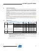
9.2. Standby Current
Tc = -40° to +85° C (unless otherwise noted)
(1)
V
CC
and V
CC_ANT
=
3.0 to 3.6 V
V
CC
and V
CC_ANT
=
4.5 to 5.5 V
Symbol Parameter Condition
Min
T
ypical Max Min
T
ypical Max
Units
Standby, CLKO Enabled, OSC and PLL Enabled mA
Standby, CLKO Disabled, OSC and PLL Enabled 10 15 mA
Standby, CLKO and PLL Disabled, OSC Enabled mA
ISB
Power Supply Standby Current
Standby, CLKO, OSC and PLL Disabled mA
Standby, CLKO Enabled, OSC and PLL Enabled 2 3 mA
Standby, CLKO Disabled, OSC and PLL Enabled 1 2 mA
Standby, CLKO and PLL Disabled, OSC Enabled mA
ISB_ANT
Power Supply Standby Current
Standby, CLKO, OSC and PLL Disabled mA
Note: 1. Typical values at Tc = 35° C. Maximum values are characterized values and not test limits in production.
2. Total power supply standby current is ISB + ISB_ANT
3. The Sleep Command is sent to enter standby mode. All serial interface signal must remain unchanged to
remain in standby mode.
4. PLL Register bits control standby mode options: ENB controls CLKO, SL1 controls PLL, SL2 controls
OSC (crystal oscillator)
5. Supply current is dependent on the reader circuit design, PCB layout, and component specifications. All
values in table measured on an Atmel reference design.
All values are preliminary and will be updated after characterization.
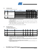
9.3. RF Characteristics
Transmitter Characteristics
Tc = -40° to +85° C (unless otherwise noted)
(1)
Symbol Parameter Condition
Min Typical Max Units ISO / IEC Standard
fc Carrier Frequency
(3)
RF Enabled
13.553 13.560 13.567 MHz
14443-2 6.1
M.I. Field Modulation Index
(4)
RF Enabled, Transmitting Data
8 11 14 percent
14443-2 9.1.2
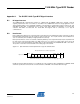
ETU Elementary Time Unit RF Enabled, Transmitting Data
9.4346 9.4395 9.4444 uS
14443-2 9.1.1
EGT Extra Guard Time RF Enabled, Transmitting Data
0 0 0 uS
14443-3 7.1.2
H Unmodulated Magnetic Field
(5)
RF Enabled, Idle
A/m rms
14443-2 6.2
Note: 1. Typical values at Tc = 35° C. Values are characterized values and not test limits in production.
2. Performance is dependent on the reader circuit design, PCB layout, and component specifications. All
values in table measured on an Atmel reference design.
3. Operating Frequency is dependent on the reader circuit design, PCB layout, and component
specifications. An Atmel reference design with 13.560 MHz 50 ppm crystal was used to characterize this
parameter.
4. Modulation Index is determined by the ML bit setting in the TXC register.
5. Unmodulated Magnetic Field strength is different for each reader antenna and reader board design. See
AT88RF1354 Application Notes.