
Manual

20 13.56 MHz Type B RF Reader
8547A−RFID−10/08
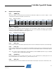
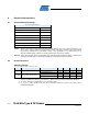
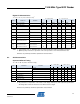
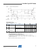
CLKO Output Timing
Tc = -40° to +85° C (unless otherwise noted)
(1)
V
CC
= 3.0 to 3.6 V V
CC
= 4.5 to 5.5 V
Symbol Parameter Condition
Min Typical Max Min Typical Max
Units
PLL Reg RS1 = 0 b RS2 = 0 b 1.978 1.978 MHz
PLL Reg RS1 = 0 b RS2 = 1 b 3.955 3.955 MHz
PLL Reg RS1 = 1 b RS2 = 0 b 7.910 7.910 MHz
f
CLKO
CLKO Output Frequency
(2)
PLL Reg RS1 = 1 b RS2 = 1 b 15.820 15.820 MHz
CLKO Duty Cycle 50.0 50.0 %
t
R_CLKO
Rise Time nS
t
F_CLKO
Fall Time nS
Note: 1. Typical values at 25° C. Values are characterized values and not test limits in production.
2. Operating Frequency is dependent on the reader circuit design, PCB layout, and component
specifications. An Atmel reference design with 13.560 MHz 50 ppm crystal was used to characterize this
parameter.
All values are preliminary and will be updated after characterization