
Manual

18 13.56 MHz Type B RF Reader
8547A−RFID−10/08
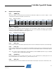
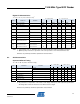
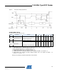
TWI Mode Timing
Tc = -40° to +85° C (unless otherwise noted)
(1)
100 kHz Operation 1 MHz Operation
Symbol Parameter Condition
Min Typical Max Min Typical Max
Unit
s
t
HIGH
SCK High pulse width
4.0 0.4 uS
t
LOW
SCK Low pulse width
4.7 0.5 uS
t
SU;DAT
Setup time, Data
250 25 nS
t
HD;DAT
Hold time, Data
300 30 nS
t
SU;STA
Setup time, Start condition
4.7 0.5 uS
t
HD;STA
Hold time, Start condition
4.0 0.4 uS
t
SU;STO
Setup time, Stop Condition
4.0 0.4 uS
t
r
Rise Time of SCK and SDA
1000 100 nS
t
f
Fall time of SCK and SDA
300 30 nS
C
b
Bus Capacitance for each bus line
400 100 pF
Note: 1. Typical values at 25° C. Maximum values are characterized values and not test limits in production.
2. Production test is performed with 50% duty cycle clock at 1 MHz.
3. Timing limits for clock frequencies less than 1 MHz are scaled with the clock frequency.
All values are preliminary and will be updated after characterization.
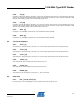
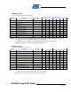
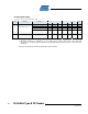
SPI Mode Timing
Tc = -40° to +85° C (unless otherwise noted)
(1)
V
CC
= 3.0 to 3.6 V V
CC
= 4.5 to 5.5 V
Symbol Parameter Condition
Min Typical Max Min Typical Max
Unit
s
t
HIGH
SCK High pulse width
See 11 in Figure 5. 250 250 nS
t
LOW
SCK Low pulse width See 11 in Figure 5.
250 250 nS
t
SETUP
MOSI (SDI) Setup to SCK High See 13 in Figure 5.
10 20 nS
t
HOLD
MOSI (SDI) Hold after SCK High See 14 in Figure 5.
100 100 nS
t
VALID
SCK Low to MISO (SDO) Valid See 15 in Figure 5.
15 15 nS
t
SSBW
SCK Low to SSB High See 16 in Figure 5.
20 20 nS
t
SSBO
SSB Low to MISO (SDO) Out See 9 in Figure 5.
15 15 nS
t
r
Rise time of all signals See 12 in Figure 5.
1600 1600 nS
t
f
Fall time of all signals See 12 in Figure 5.
1600 1600 nS
t
TRIO
SSB High to MISO (SDO) Tristate See 17 in Figure 5.
10 10 nS
Note: 1. Typical values at 25° C. Maximum values are characterized values and not test limits in production.
2. Production test is performed with 50% duty cycle clock at 1 MHz.
All values are preliminary and will be updated after characterization.