
Manual

13.56 MHz Type B RF Reader
17
8547A−RFID−10/08
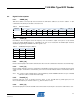
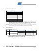
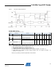
Digital I/O Characteristics
Tc = -40° to +85° C (unless otherwise noted)
(1)
V
CC
= 3.0 to 3.6 V V
CC
= 4.5 to 5.5 V
Symbol Parameter Condition
Min Typical Max Min
Typ
ical
Max
Units
V
IL
Input Low Voltage
-0.5 0.3V
CC
-0.5 0.3V
CC
V
V
IH
Input High Voltage
0.7V
CC
V
CC
+0.5 0.7V
CC
V
CC
+0.5 V
V
OL
Output Low Voltage
(except SDI pin in TWI mode)
V
CC
= max
I
OL
= mA
V
V
OH
Output High Voltage
(except SDI pin in TWI mode)
V
CC
= max
I
OH
= mA
V
V
OL1
Output Low Voltage
(SDI pin TWI mode only)
V
CC
= max
I
OL
= 3 mA
0 0.4 0 0.4 V
I
IL
Input Low Leakage Current V
CC
= max, pin low
uA
I
IH
Input High Leakage Current V
CC
= max, pin high
uA
TWI mode, SCK = 100kHz
1.0 4.0 1.7 8.0 kOhm
R
SDA
I/O pin Pull-up Resistor
(2)
TWI mode, SCK = 1 MHz
1.0 2.0 1.7 3.3 kOhm
R
RST
ResetB Pull-up Resistor
kOhm
R
PU
Input Pull-up Resistor Unused input pin
kOhm
R
PD
Input Pull-down Resistor Unused input pin
0 0 kOhm
Note: 1. Typical values at 25° C. Maximum values are characterized values and not test limits in production.
2. Optimum pull-up resistance is dependent on the total capacitance of the TWI serial interface bus.
All Values are preliminary and will be updated after characterization.
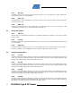
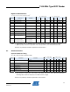
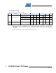
8.3. AC Characteristics
System and Reset Timing
Tc = -40° to +85° C (unless otherwise noted)
(1)
V
CC
= 3.0 to 3.6 V V
CC
= 4.5 to 5.5 V
Symbol Parameter Condition
Min Typical Max Min Typical Max
Units
TWI mode 1.0 1.0 MHz
f
SCK
Serial Interface Clock Frequency
SPI mode 2.0 2.0 MHz
t
RST
Minimum pulse width on ResetB Pin
500 500 uS
t
OSC
Crystal Oscillator start-up time
At power-up 1000 1000 uS
t
RF_ON
RF Enable time
(2)
From end of command to RF 90% power 4.5 1.8 uS
t
RF_OFF
RF Disable time
(2)
From end of command to RF 10% power 1.7 1.7 uS
t
CLKO
CLKO start-up time
At power-up uS
Note: 1. Typical values at 25° C. Maximum values are characterized values and not test limits in production.
2. RF performance is dependent on the reader circuit design, PCB layout, and component specifications.
RF timing values in table are measured on an Atmel reference design.
All values are preliminary and will be updated after characterization.