
Manual

13.56 MHz Type B RF Reader
13
8547A−RFID−10/08
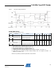
6.4.5. C5 [6]
C5 bypass capacitor pin. Bypass capacitance of 0.33 uF for the digital circuits must be connected between the C5 pin
and V
SS
. This capacitor must be placed within 3 mm of the package. Any 0.33 uF ceramic capacitor with X5R or X7R
dielectric and a working voltage of 10 volts minimum may be used.
6.4.6. C7 [29]
C7 bypass capacitor pin. Bypass capacitance of 47 nF for the analog circuits must be connected between the C7 pin
and V
SS
A. This capacitor must be placed within 3 mm of the package. Any 47 nF ceramic capacitor with X5R or X7R
dielectric and a working voltage of 10 volts minimum may be used.
6.4.7. Xtal1 [4]
Crystal pin 1. A 13.56 MHz crystal must be connected between Xtal1 and Xtal2.
6.4.8. Xtal2 [5]
Crystal pin 2. A 13.56 MHz crystal must be connected between Xtal1 and Xtal2.
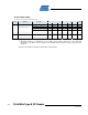
6.5. Test Pin Descriptions
6.5.1. Test1 [7]
Test input pin 1. This pin must be connected to V
SS
on the board to prevent the IC from entering test mode.
6.5.2. Test2 [16]
Test input pin 2. This pin must be connected to V
SS
on the board to prevent the IC from entering test mode.
6.5.3. Test3 [17]
Test input pin 3. This pin must be connected to V
SS
on the board to prevent the IC from entering test mode.
6.5.4. TestD [11]
Test output pin D. This test output must be left open by the user.
6.5.5. TestR [31]
Test output pin R. This test output must be left open by the user.
6.5.6. Rmod [34]
Test pin Rmod. This pin must be connected to V
SS
_Ant on the board.
6.6. Other Pins
6.6.1. N.C. [18, 28, 30, 33, 36]
No Connect pins. These package pins are not used and can be left open by the user.