
User Manual


43
8111A–AVR–05/08
AT86RF231
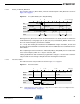
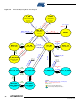
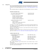
The state transition timing is calculated based on the timing of the individual blocks shown in
Figure 7-3 on page 39 to Figure 7-7 on page 41. The worst case values include maximum oper-
ating temperature, minimum supply voltage, and device parameter variations.
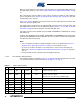
10 t
TR10
PLL_ON BUSY_TX 16
When asserting pin 11 (SLP_TR) or TRX_CMD = TX_START
first symbol transmission is delayed by 16 µs delay (PLL
settling and PA ramp up)
11 t
TR11
BUSY_TX PLL_ON 32 PLL settling time from TX_BUSY to PLL_ON state
12 t
TR12
All modes TRX_OFF 1
Using TRX_CMD = FORCE_TRX_OFF (see register 0x02,
TRX_STATE),
Not valid for SLEEP state
13 t
TR13
RESET TRX_OFF 37 Valid for P_ON or SLEEP state
14 t
TR14
Various
States
PLL_ON 1
Using TRX_CMD = FORCE_PLL_ON (see register 0x02,
TRX_STATE),
Not valid for SLEEP, P_ON, RESET, TRX_OFF and *_NO_CLK
Table 7-1. State Transition Timing (Continued)
No Symbol Transition Time [µs], (type) Comments
⇒
⇒
⇒
⇒
⇒
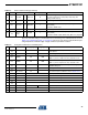
Table 7-2. Analog Block Initialization and Settling Time
No Symbol Block Time [µs], (type) Time [µs], (max) Comment
15 t
TR15
XOSC 215 1000
Leaving SLEEP state, depends on crystal Q factor and
load capacitor
16 t
TR16
FTN 25 FTN tuning time fixed
17 t
TR17
DVREG 60 1000
Depends on external bypass capacitor at DVDD
(CB3 = 1 µF nom., 10 µF worst case), depends on V
DD
18 t
TR18
AVREG 60 1000
Depends on external bypass capacitor at AVDD
(CB1 = 1 µF nom, 10 µF worst case), depends on V
DD
19 t
TR19
PLL, initial 110 155
PLL settling time TRX_OFF PLL_ON, including 60 µs
AVREG settling time
20 t
TR20
PLL settling 11 24 Settling time between channels switch
21 t
TR21
PLL, CF cal 35 PLL center frequency calibration, refer to Section 9.7.4
22 t
TR22
PLL, DCU cal 6 PLL DCU calibration, refer to Section 9.7.4
23 t
TR23
PLL, RX TX 16 Maximum PLL settling time RX TX
24 t
TR24
PLL, TX RX 32 Maximum PLL settling time TX RX
25 t
TR25
RSSI, update 2 RSSI update period in receive states, refer to Section 8.3.2
26 t
TR26
ED 140 ED measurement period, refer to Section 8.4.2
27 t
TR27
SHR, sync 96 Typical SHR synchronisation period, refer to Section 8.4.2
28 t
TR28
CCA 140 CCA measurement period, refer to Section 8.5.2
29 t
TR29
Random value 1 Random value update period, refer to Section 11.2.1
⇒
⇒ ⇒
⇒ ⇒