
User Manual


39
8111A–AVR–05/08
AT86RF231
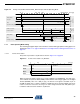
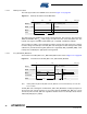
Figure 7-2. Timing of RX_START, AMI and TRX_END Interrupts in Basic Operating Mode
7.1.4 Basic Operating Mode Timing
The following paragraphs depict state transitions and their timing properties. Timing figures are
explained in Table 7-1 on page 42 and Section 12.4 “Digital Interface Timing Characteristics” on
page 157.
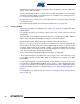
7.1.4.1 Power-on Procedure
The power-on procedure to P_ON state is shown in Figure 7-3 on page 39.
Figure 7-3. Power-on Procedure to P_ON State
When the external supply voltage (V
DD
) is firstly supplied to the AT86RF231, the radio trans-
ceiver enables the crystal oscillator (XOSC) and the internal 1.8V voltage regulator for the digital
domain (DVREG). After t
TR1
= 380 µs (typ.), the master clock signal is available at pin 17
(CLKM) at default rate of 1 MHz. If CLKM is available the SPI is already enabled and can be
used to control the transceiver. As long as no state change towards state TRX_OFF is per-
formed the radio transceiver remains in P_ON state.
128 160 1920 192+(9+m)*32-16 Time [µs]
RX
(Device 2)
IRQ_2 (RX_START)
RX_ON RX_ON
IRQ
TRX_STATE
Interrupt latency
TRX_ENDIRQ_5 (AMI)
t
IRQ
BUSY_RX
IRQ_3 (TRX_END)
TX
(Device1)
PLL_ON BUSY_TX PLL_ON
IRQ
SLP_TR
TRX_STATE
Typ. Processing Delay
16 µs
Frame
on Air
Preamble
SFD PHR
MSDU
411 mNumber of Octets
Frame Content
MHR
7
FCS
2
t
IRQ
t
IRQ
0
Event
State
V
DD
on
P_ON
Block
XOSC, DVREG
100
CLKM on
400 Time [µs]
Time
t
TR1