
User Manual


38
8111A–AVR–05/08
AT86RF231
A reset forces the radio transceiver into TRX_OFF state. If the device is still in the P_ON state it
remains in the P_ON state though.
A reset is initiated with pin /RST = L and the state is left after setting /RST = H. The reset pulse
should have a minimum length as specified in Section 12.4 “Digital Interface Timing Characteris-
tics” on page 157 see parameter 12.4.13.
During reset the microcontroller has to set the radio transceiver control pins SLP_TR and /SEL
to their default values.
An overview about the register reset values is provided in Table 14-1 on page 167.
7.1.3 Interrupt Handling
All interrupts provided by the AT86RF231 (see Table 6-9 on page 29) are supported in Basic
Operating Mode.
For example, interrupts are provided to observe the status of radio transceiver RX and
TX operations.
On receive IRQ_2 (RX_START) indicates the detection of a valid PHR first, IRQ_5 (AMI) an
address match and IRQ_3 (TRX_END) the completion of the frame reception.
On transmit IRQ_3 (TRX_END) indicates the completion of the frame transmission.
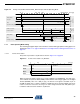
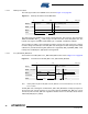
Figure 7-2 on page 39 shows an example for a transmit/receive transaction between two
devices and the related interrupt events in Basic Operating Mode. Device 1 transmits a frame
containing a MAC header (in this example of length 7), payload and valid FCS. The frame is
received by Device 2 which generates the interrupts during the processing of the incoming
frame. The received frame is stored in the Frame Buffer.
The first interrupt IRQ_2 (RX_START) signals the reception of a valid PHR.
If the received frame passes the address filter, refer to Section 7.2.3.5 “Frame Filtering” on page
61, an address match interrupt IRQ_5 (AMI) is issued after the reception of the MAC
header (MHR).
In Basic Operating Mode the third interrupt IRQ_3 (TRX_END) is issued at the end of the
received frame. In Extended Operating Mode, refer to Section 7.2 “Extended Operating Mode”
on page 47; the interrupt is only issued if the received frame passes the address filter and the
FCS is valid. Further exceptions are explained in Section 7.2 “Extended Operating Mode” on
page 47.
Processing delay
f
IRQ
is a typical value, refer to Section 12.4 “Digital Interface Timing Character-
istics” on page 157.