
User Manual


23
8111A–AVR–05/08
AT86RF231
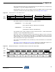
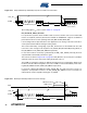
On SRAM write access, one or more bytes of write data are transferred on MOSI starting with
the third byte of the access sequence (see Figure 6-12 on page 23).
On SRAM read or write accesses do not attempt to read or write bytes beyond the SRAM buffer
size.
Figure 6-12. Packet Structure - SRAM Write Access
As long as /SEL = L, every subsequent byte read or byte write increments the address counter
of the Frame Buffer until the SRAM access is terminated by /SEL = H.
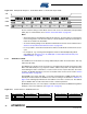
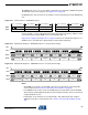
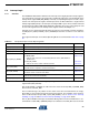
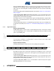
Figure 6-13 on page 23 and Figure 6-14 on page 23 illustrate an example SPI sequence of a
SRAM access to read and write a data package of 5-byte length respectively.
Figure 6-13. Example SPI Sequence - SRAM Read Access of a 5 byte Data Package
Figure 6-14. Example SPI Sequence - SRAM Write Access of a 5 byte Data Package
Notes
• The SRAM access mode is not intended to be used as an alternative to the Frame Buffer
access modes (see Section 6.2.2 “Frame Buffer Access Mode” on page 20).
• If the SRAM access mode is used to read PSDU data, the Frame Buffer contains all PSDU
data except the frame length byte (PHR). The frame length information can be accessed only
using Frame Buffer access.
• Frame Buffer access violations are not indicated by a TRX_UR interrupt when using the
SRAM access mode, for further details refer to Section 9.3.3 “Interrupt Handling” on page
109.
0 reserved[5:0]1MOSI
PHY_STATUSMISO
byte 1 (command byte)
0 ADDRESS[7:0]
XX
byte 2 (address)
DATA[7:0]
XX
byte 3 (data byte)
DATA[7:0]
XX
byte n-1 (data byte)
DATA[7:0]
XX
byte n (data byte)
COMMAND ADDRESS XX XX XX XX
PHY_STATUS XX DATA 2DATA 1 DATA 4DATA 3
XX
DATA 5
SCLK
MOSI
MISO
/SEL
COMMAND ADDRESS DATA 1 DATA 2 DATA 3 DATA 4
PHY_STATUS XX XXXX XXXX
DATA 5
XX
SCLK
MOSI
MISO
/SEL