
User Manual


20
8111A–AVR–05/08
AT86RF231
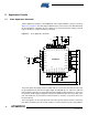
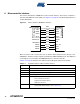
Figure 6-5. Packet Structure - Register Write Access
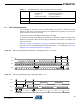
Each register access must be terminated by setting /SEL = H.
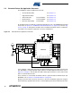
Figure 6-6 on page 20 illustrates a typical SPI sequence for a register access sequence for write
and read respectively.
Figure 6-6. Example SPI Sequence - Register Access Mode
6.2.2 Frame Buffer Access Mode
The 128 byte Frame Buffer can hold the PHY service data unit (PSDU) data of one
IEEE 802.15.4 compliant RX or one TX frame of maximum length at a time. A detailed descrip-
tion of the Frame Buffer can be found in Section 9.3 “Frame Buffer” on page 107. An introduction
to the IEEE 802.15.4 frame format can be found in Section 8.1 “Introduction - IEEE 802.15.4 -
2006 Frame Format” on page 79.
Frame Buffer read and write accesses are used to read or write frame data (PSDU and addi-
tional information) from or to the Frame Buffer. Each access starts with /SEL = L followed by a
command byte on MOSI. If this byte indicates a frame read or write access, the next byte
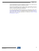
PHR[7:0] indicates the frame length followed by the PSDU data, see Figure 6-7 on page 20 and
Figure 6-8 on page 21.
On Frame Buffer read access, PHY header (PHR) and PSDU are transferred via MISO starting
with the second byte. After the PSDU data, one more byte is transferred containing the link qual-
ity indication (LQI) value of the received frame, for details refer to Section 8.6 “Link Quality
Indication (LQI)” on page 99. Figure 6-7 on page 20 illustrates the packet structure of a Frame
Buffer read access.
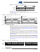
Figure 6-7. Packet Structure - Frame Read Access
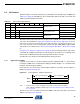
1 ADDRESS[5:0]1 WRITE DATA[7:0]MOSI
PHY_STATUS XXMISO
byte 1 (command byte) byte 2 (data byte)
PHY_STATUS XX PHY_STATUS READ DATA
WRITE COMMAND WRITE DATA READ COMMAND XX
Register Write Access Register Read Access
SCLK
MOSI
MISO
/SEL
0 reserved[5:0]0MOSI
PHY_STATUSMISO
byte 1 (command byte)
1 XX
PHR[7:0]
byte 2 (data byte)
XX
PSDU[7:0]
byte 3 (data byte)
XX
PSDU[7:0]
byte n-1 (data byte)
XX
LQI[7:0]
byte n (data byte)