
User Manual


19
8111A–AVR–05/08
AT86RF231
6.2 SPI Protocol
Each SPI sequence starts with transferring a command byte from the SPI master via MOSI (see
Table 6-2 on page 19) with MSB first. This command byte defines the SPI access mode and
additional mode-dependent information.
Each SPI transfer returns bytes back to the SPI master on MISO. The content of the first byte
(see value "PHY_STATUS" in Figure 6-4 on page 19 to Figure 6-14 on page 23) is set to zero
after reset. To transfer status information of the radio transceiver to the microcontroller, the con-
tent of the first byte can be configured with register bits SPI_CMD_MODE (register 0x04,
TRX_CTRL_1). For details, refer to Section 6.3.1 “Register Description - SPI Control” on page
24.
In Figure 6-4 on page 19 to Figure 6-14 on page 23 and the following chapters logic values
stated with XX on MOSI are ignored by the radio transceiver, but need to have a valid logic level.
Return values on MISO stated as XX shall be ignored by the microcontroller.
The different access modes are described within the following sections.
6.2.1 Register Access Mode
A register access mode is a two-byte read/write operation initiated by /SEL = L. The first trans-
ferred byte on MOSI is the command byte including an identifier bit (bit7 = 1), a read/write select
bit (bit 6), and a 6-bit register address.
On read access, the content of the selected register address is returned in the second byte on
MISO (see Figure 6-4 on page 19).
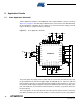
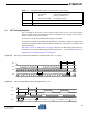
Figure 6-4. Packet Structure - Register Read Access
Note: 1. Each SPI access can be configured to return radio controller status information
(PHY_STATUS) on MISO, for details refer to Section 6.3 “Radio Transceiver Status informa-
tion” on page 24.
On write access, the second byte transferred on MOSI contains the write data to the selected
address (see Figure 6-6 on page 20).
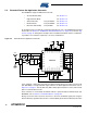
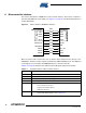
Table 6-2. SPI Command Byte definition
Bit 7 Bit 6 Bit 5 Bit 4 Bit 3 Bit 2 Bit 1 Bit 0 Access Mode Access Type
1 0 Register address [5:0]
Register access
Read access
1 1 Register address [5:0] Write access
001 Reserved
Frame Buffer access
Read access
0 1 1 Reserved Write access
000 Reserved
SRAM access
Read access
0 1 0 Reserved Write access
1 ADDRESS[5:0]0 XXMOSI
PHY_STATUS
(1)
READ DATA[7:0]MISO
byte 1 (command byte) byte 2 (data byte)