
User Manual


158
8111A–AVR–05/08
AT86RF231
Notes: 1. Maximum pulse width less than (TX frame length + 16 µs)
2. For Fast SRAM read/write accesses on address space 0x82 - 0x94 the time t
5
(Min.) increases to 450 ns.
12.5 General RF Specifications
Test Conditions (unless otherwise stated):
V
DD
= 3.0V, f
RF
= 2.45 GHz, T
OP
= 25°C, Measurement setup see Figure 5-1 on page 12.
Note: 1. A reference frequency accuracy of ±40 ppm is required by [1], [2].
12.4.15 t
12
AES core cycle time 24 µs
12.4.16 t
IRQ
Interrupt event latency Relative to the event to be indicated 9 µs
12.4.17 f
CLKM
Clock frequency at pin 17 (CLKM) Configurable in register 0x03
(TRX_CTRL_0)
0
1
2
4
8
16
250
62.5
MHz
MHz
MHz
MHz
MHz
MHz
kHz
kHz
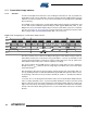
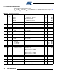
Table 12-4. Digital Interface Timing Characteristics (Continued)
Table 12-5. General RF Specifications
No. Symbol Parameter Condition Min. Typ. Max Units
12.5.1 f
RF
Frequency range As specified in [1], [2] 2405 2480 MHz
12.5.2 f
CH
Channel spacing As specified in [1], [2] 5MHz
12.5.3 f
HDR
Header bit rate (SHR, PHR) As specified in [1], [2] 250 kb/s
12.5.4 f
PSDU
PSDU bit rate As specified in [1], [2]
OQPSK_DATA_RATE = 1
OQPSK_DATA_RATE = 2
OQPSK_DATA_RATE = 3
250
500
1000
2000
kb/s
kb/s
kb/s
kb/s
12.5.5 f
CHIP
Chip rate As specified in [1], [2] 2000 kchip/s
12.5.6 f
CLK
Crystal oscillator frequency Reference oscillator 16 MHz
12.5.7 f
XTAL
Reference oscillator settling time Leaving SLEEP state to clock
available at pin 17 (CLKM)
215 1000 µs
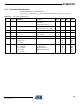
12.5.8 Symbol rate deviation
Reference frequency accuracy for
correct functionality
PSDU bit rate 250 kb/s
PSDU bit rate 500 kb/s
PSDU bit rate 1000 kb/s
PSDU bit rate 2000 kb/s
-60
(1)
-40
-40
-30
+60
+40
+40
+30
ppm
ppm
ppm
ppm
12.5.9 B
20dB
20 dB bandwidth 2.8 MHz