
User Manual


157
8111A–AVR–05/08
AT86RF231
12.3 Digital Pin Characteristics
.Test Conditions: T
OP
= 25°C (unless otherwise stated)
Note: 1. The capacitive load should not be larger than 50 pF for all I/Os when using the default driver strength settings, refer to Sec-
tion 1.3.1 “Driver Strength Settings” on page 7. Generally, large load capacitances increase the overall current consumption.
12.4 Digital Interface Timing Characteristics
Test Conditions: T
OP
= 25°C, V
DD
= 3.0V, C
L
= 50 pF (unless otherwise stated).
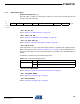
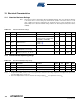
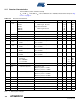
Table 12-3.
Digital Pin Characteristics
No. Symbol Parameter Condition Min. Typ. Max Units
12.3.1 V
IH
High level input voltage
(1)
V
DD
- 0.4 V
12.3.2 V
IL
Low level input voltage
(1)
0.4 V
12.3.3 V
OH
High level output voltage
(1)
For all output driver strengths defined
in TRX_CTRL_0
V
DD
- 0.4 V
12.3.4 V
OL
Low level output voltage
(1)
For all output driver strengths defined
in TRX_CTRL_0
0.4 V
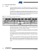
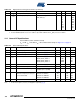
Table 12-4. Digital Interface Timing Characteristics
No. Symbol Parameter Condition Min. Typ. Max Units
12.4.1 f
sync
SCLK frequency synchronous operation 8 MHz
12.4.2 f
async
SCLK frequency asynchronous operation 7.5 MHz
12.4.3 t
1
/SEL low to MISO active 180 ns
12.4.4 t
2
SCLK to MISO out data hold time 25 ns
12.4.5 t
3
MOSI setup time 10 ns
12.4.6 t
4
MOSI hold time 10 ns
12.4.7 t
5
LSB last byte to MSB next byte 250
(2)
ns
12.4.8 t
6
/SEL high to MISO tri state 10 ns
12.4.9 t
7
SLP_TR pulse width TX start trigger 62.5 Note
(1)
ns
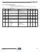
12.4.10 t
8
SCLK to /SEL high SPI Read/Write, standard SRAM
and Frame Buffer access modes,
Idle time between consecutive SPI
accesses
250 ns
12.4.11 t
8
SCLK to /SEL high Fast SRAM read/write access
mode, refer to Section 11.1.5,
Idle time between consecutive SPI
accesses
500 ns
12.4.12 t
9
Last SCLK to /SEL high 250 9 ns
12.4.13 t
10
Reset pulse width ≥ 10 clock cycles at 16 MHz 625 ns
12.4.14 t
11
SPI access latency after reset ≥ 10 clock cycles at 16 MHz 625 ns