
User Manual


148
8111A–AVR–05/08
AT86RF231
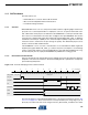
to the transmit frequency within 16 µs. The modulation starts 16 µs after the rising edge of
SLP_TR. During this time, the PA buffer and the internal PA are enabled.
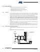
The control of an external PA is done via differential pin pair DIG3/DIG4. DIG3 = H / DIG4 = L
indicates that the transmission starts and can be used to enable an external PA. The timing of
pins DIG3/DIG4 can be adjusted relative to the start of the frame and the activation of the inter-
nal PA buffer. This is controlled using register bits PA_BUF_LT and PA_LT. For details refer to
Section 9.2.4 “TX Power Ramping” on page 104.
11.5.3 Register Description
Register 0x04 (TRX_CTRL_1):
The TRX_CTRL_1 register is a multi purpose register to control various operating modes and
settings of the radio transceiver.
• Bit 7 - PA_EXT_EN
This register bit enables pin 1 (DIG3) and pin 2 (DIG4) to indicate the transmit state of the radio
transceiver.
Note: 1. It is recommended to set PA_EXT_EN = 1 only in receive or transmit states to reduce the
power consumption or avoid leakage current of external RF switches or other building blocks,
especially during SLEEP state.
• Bit 6 - IRQ_2_EXT_EN
Refer to Section 11.6 “RX Frame Time Stamping” on page 150.
• Bit 5 - TX_AUTO_CRC_ON
Refer to Section 8.2 “Frame Check Sequence (FCS)” on page 85.
• Bit 4 - RX_BL_CTRL
Refer to Section 11.7 “Frame Buffer Empty Indicator” on page 152.
• Bit [3:2] - SPI_CMD_MODE
Refer to Section 6.3 “Radio Transceiver Status information” on page 24.
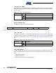
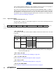
Bit 7 6 5 4 3 2 1 0
+0x04 PA_EXT_EN IRQ_2_EXT_EN TX_AUTO_CRC_ON RX_BL_CTRL SPI_CMD_MODE IRQ_MASK_MODE IRQ_POLARITY TRX_CTRL_1
Read/Write R/W R/W R/W R/W R/W R/W R/W
Reset Value 0 0 1 0 0 0 0
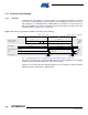
Table 11-15. RF Front-End Control Pins
PA_EXT_EN State Pin Value Description
0
n/a DIG3 L External RF front-end control disabled
DIG4 L
1
(1)
TX_BUSY DIG3 H External RF front-end control enabled
DIG4 L
Other DIG3 L
DIG4 H