
User Manual


14
8111A–AVR–05/08
AT86RF231
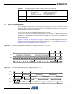
5.2 Extended Feature Set Application Schematic
The AT86RF231 supports additional features like:
An extended feature set application schematic illustrating the use of the AT86RF231 Extended
Feature Set, see Section 11. “AT86RF231 Extended Feature Set” on page 128, is shown in Fig-
ure 5-2 on page 14. Although this example shows all additional hardware features combined, it
is possible to use all features separately or in various combinations.
Figure 5-2. Extended Feature Application Schematic
In this example, a balun (B1) transforms the differential RF signal at the radio transceiver RF
pins (RFP/RFN) to a single ended RF signal, similar to the Basic Application Schematic; refer to
Figure 5-1 on page 12. The RF-Switches (SW1, SW2) separate between receive and transmit
path in an external RF front-end.
These switches are controlled by the RX/TX Indicator, represented by the differential pin pair
DIG3/DIG4, refer to Section 11.5 “RX/TX Indicator” on page 147.
During receive the radio transceiver searches for the most reliable RF signal path using the
Antenna Diversity algorithm. One antenna is selected (SW2) by the Antenna Diversity RF switch
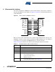
•
Security Module (AES) see Section 11.1
•
High Data Rate Mode see Section 11.3
•
Antenna Diversity uses pins DIG1/2 see Section 11.4
•
RX/TX indicator uses pins DIG3/4 see Section 11.5
•
RX Frame Time Stamp uses pin DIG2 see Section 11.6
8
7
6
5
4
3
2
1
9 10111213141516
2526
2728
2930
3132
AT86RF231
DIG3
AVSS
DIG4
AVSS
AVSS
RFP
RFN
AVSS
DVSS
DIG1
DIG2
SLP_TR
DVSS
DVDD
DVDD
XTAL2
DEVDD
DVSS
AVSS
AVDD
EVDD
AVSS
XTAL1
17
18
19
20
21
22
23
24
DVSS
CLKM
IRQ
MISO
DVSS
MOSI
SCLK
CB3 CB4
XTAL
CX1 CX2
CB1
Digital Interface
V
DD
/RST
/SEL
Balun
RF-
Switch
ANT0
ANT1
RF-
Switch
B1SW1
SW2
V
DD
CB2
C3
R1
PA
LNA
N1
N2