
User Manual


12
8111A–AVR–05/08
AT86RF231
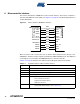
5. Application Circuits
5.1 Basic Application Schematic
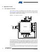
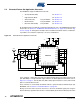
A basic application schematic of the AT86RF231 with a single-ended RF connector is shown in
Figure 5-1 on page 12. The 50Ω single-ended RF input is transformed to the 100Ω differential
RF port impedance using balun B1. The capacitors C1 and C2 provide AC coupling of the RF
input to the RF port, capacitor C4 improve matching.
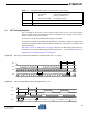
Figure 5-1. Basic Application Schematic
The power supply decoupling capacitors (CB2, CB4) are connected to the external analog sup-
ply pin (EVDD, pin 28) and external digital supply pin (DEVDD, pin 15). Capacitors CB1 and
CB3 are bypass capacitors for the integrated analog and digital voltage regulators to ensure sta-
ble operation. All decoupling and bypass capacitors should be placed as close as possible to the
pins and should have a low-resistance and low-inductance connection to ground to achieve the
best performance.
The crystal (XTAL), the two load capacitors (CX1, CX2), and the internal circuitry connected to
pins XTAL1 and XTAL2 form the crystal oscillator. To achieve the best accuracy and stability of
8
7
6
5
4
3
2
1
9
10 11
12
13 14
15 16
2526272829303132
AT86RF231
DIG3
AVSS
DIG4
AVSS
AVSS
RFP
RFN
AVSS
DVSS
DIG1
DIG2
SLP_TR
DVSS
DVDD
DVDD
XTAL2
DEVDD
DVSS
AVSS
AVDD
EVDD
AVSS
XTAL1
17
18
19
20
21
22
23
24
DVSS
CLKM
IRQ
MISO
DVSS
MOSI
SCLK
CB3 CB4
Digital Interface
/RST
/SEL
V
DD
XTAL
CX1 CX2
CB1
V
DD
CB2
C1
C2
B1
RF
C3
R1
C4