
User Manual

105
8111A–AVR–05/08
AT86RF231
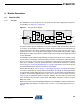
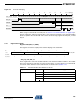
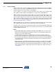
Figure 9-3. TX Power Ramping
When using an external RF front-end (refer to Section 11.5 “RX/TX Indicator” on page 147) it
may be required to adjust the startup time of the external PA relative to the internal building
blocks to optimize the overall PSD. This can be achieved using register bits PA_BUF_LT and
PA_LT.
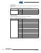
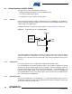
9.2.5 Register Description
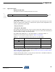
Register 0x05 (PHY_TX_PWR):
This register controls the output power and the ramping of the transmitter.
• Bit [7:6] - PA_BUF_LT
These register bits control the enable lead time of the internal PA buffer relative to the enable
time of the internal PA. This time is further used to derive a control signal for an external RF
front-end to switch between receive and transmit, for details refer to Section 11.5.
0 6810
SLP_TR
TRX_STATE PLL_ON
2
12 14 16 18
Length [µs]
PA buffer
4
PA
PA_BUF_LT
PA_LT
Modulation 11 11 11000
BUSY_TX
Bit 7 6 5 4 3 2 1 0
+0x05 PA_BUF_LT PA_LT TX_PWR PHY_TX_PWR
Read/Write R/W R/W R/W R/W R/W R/W R/W R/W
Reset Value 1 1 0 0 0 0 0 0
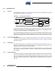
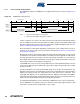
Table 9-2. PA Buffer Enable Time Relative to the PA
Register Bits Value PA Buffer Lead Time [µs]
PA_BUF_LT 0 0
12
24
3 6