
Manual

7
AT86RF230
5131A-ZIGB-06/14/06
No Parameter Symbol
Min Typ Max Unit Conditions/Notes
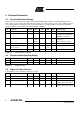
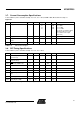
3.3.5 Controller clock frequency
(CLKM)
f
CLKM
0
1
2
4
8
16
MHz
MHz
MHz
MHz
MHz
MHz
Programmable in register
TRX_CTRL_0
Table 3-3. Digital Pin Specifications
The capacitive load should not be larger than 50 pF for all I/Os when using the default driver strength settings.
Generally, large load capacitances will increase the overall current consumption.
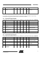
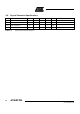
3.4. General RF Specifications
Test Conditions (unless otherwise stated): V
dd
= 3V, f = 2.45 GHz, T
amb
= 25°C, Measurement setup see Figure 9-1
No Parameter Symbol
Min Typ Max Unit Conditions/Notes
3.4.1 Frequency range f
2405 2480 MHz
3.4.2 Bit rate f
bit
250 kbit/s As specified in [1]
3.4.3 Chip rate f
chip
2000 kchip/s
As specified in [1]
3.4.4 Reference oscillator
frequency
f
clk
16 MHz
3.4.5 Reference oscillator settling
time
0.5 1 ms Leaving SLEEP state to clock
available at pin CLKM
3.4.6 Reference frequency
accuracy for correct
functionality
-60 +60 ppm
±40 ppm is required by [1]
3.4.7 20 dB bandwidth B
20dB
2.8 MHz
Table 3-4: General RF Parameters
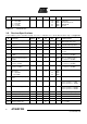
3.5. Transmitter Specifications
Test Conditions (unless otherwise stated): V
dd
= 3V, f = 2.45 GHz, T
amb
= 25°C, Measurement setup see Figure 9-1
No Parameter Symbol
Min Typ Max Unit Conditions/Notes
3.5.1 Nominal output power P
TX
0 3 6 dBm Max. value
3.5.2 Output power range 20 dB 16 steps
(register PHY_TX_PWR)
3.5.3 Output power accuracy
±3
dB
3.5.4 TX Return loss 10 dB
100Ω differential impedance,
P
TX
= 3 dBm
3.5.5 EVM 8 %rms Channel number = 20
3.5.6 Harmonics
2nd harmonic
3rd harmonic
-38
-45
dBm
dBm