
Manual

6
AT86RF230
5131A-ZIGB-06/14/06
3. Technical Parameters
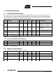
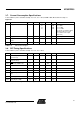
3.1. Absolute Maximum Ratings
Note: Stresses beyond those listed under “Absolute Maximum Ratings” may cause permanent damage to the
device. This is a stress rating only and functional operation of the device at these or any other conditions beyond
those indicated in the operational sections of this specifications is not implied. Exposure to absolute maximum
rating conditions for extended periods may affect device reliability.
No Parameter Symbol
Min Typ Max Unit Conditions/Notes
3.1.1 Storage temperature T
stor
-50 150 °C
3.1.2 Lead temperature T
lead
260 °C T = 10s
(soldering profile compliant with
IPC/JEDEC J-STD-020B)
3.1.3 ESD-protection V
ESD
2
200
500
kV
V
V
Compl. to [2], passed 4 kV
Compl. to [3],
Compl. to [4], passed 750V
3.1.4 Input RF level P
RF
+10 dBm
3.1.5 Voltage on all pins (except
pins 13, 14, 29)
-0.3 V
dd
+0.3
≤ 3.6
V
3.1.6 Voltage on pins 13, 14, 29 -0.3 2 V
Table 3-1. Absolute Maximum Ratings
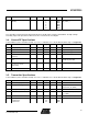
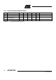
3.2. Recommended Operating Range
No Parameter Symbol
Min Typ Max Unit Conditions/Notes
3.2.1 Operating temperature range T
op
-40 +85 °C
3.2.2 Supply voltage V
dd
1.8 3.6 V
Table 3-2. Operating Range
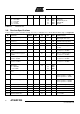
3.3. Digital Pin Specifications
Test Conditions (unless otherwise stated): T
amb
= 25°C
No Parameter Symbol
Min Typ Max Unit Conditions/Notes
3.3.1 High level input voltage V
IH
V
dd
– 0.4
V
3.3.2 Low level input voltage V
IL
0.4 V
3.3.3 High level output voltage V
OH
V
dd
– 0.4
V For all output current loads
defined in register TRX_CTR_0
3.3.4 Low level output voltage V
OL
0.4 V For all output current loads
defined in register TRX_CTR_0