
Manual

45
AT86RF230
5131A-ZIGB-06/14/06
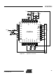
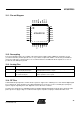
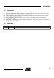
10.1. Pin-out Diagram
GND
GND
GND
RFP
RFN
GND
GND
IRQ
MOSI
GND
MISO
SCLK
GND
CLKM
GND
GND
GND
VDEC2
VDD
GND
XTAL2
XTAL1
GND
GND
SLP_TR
GND
VDEC1
VDEC1
VDD
GND
32 31 30 29 28 27 26 25
9 10 11 12 13 14 15 16
1
2
3
4
5
6
7
8
24
23
22
21
20
19
18
17
AT86RF230
RST
SEL
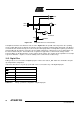
10.2. Decoupling
Correct functionality requires de-coupling of the internal power supply voltage (VDEC1/2). Capacitors of 1µF
(recommended value) shall be placed as close as possible to IC pins and shall be connected to ground with the
shortest possible traces. Avoid long lines. It is recommended to insert additional 100 nF capacitors as close as
possible at each VDD pin to ground.
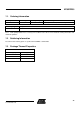
10.3. Analog Pins
Pin Condition Recommendation/Comment
RFP/RFN V
DC
= 0.9V (TX)
V
DC
= 20 mV (RX) at both pins
Blocking is required if an antenna with a DC path to ground is used.
Serial capacitance must be < 30 pF.
XTAL1/XTAL2 C
PAR
= 3 pF
V
DC
= 0.9V at both pins
Parasitic capacitance of the IC pins must be considered as additional
parallel capacitance to the crystal.
Table 10-2. Comments on RF Input/Output and Crystal Pins
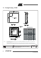
10.4. RF Pins
A differential RF input provides common-mode rejection to suppress the switching noise of the internal digital signal
processing blocks. At the board-level, the differential RF layout ensures the receiver sensitivity by rejecting any
spurious signals originating from other digital ICs such as the micro-controller.
The RF port is designed for a 100Ω differential load. A differential DC path between the RF pins is allowed. A DC
path to ground or supply voltage is not allowed and requires capacitive coupling as indicated in Table 10-2.