
Manual

44
AT86RF230
5131A-ZIGB-06/14/06
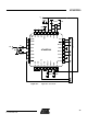
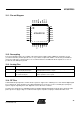
10. Pin Configuration
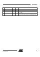
Number Name Type Description
1 GND Ground Analog ground
2 GND Ground Analog ground
3 GND Ground Ground for RF signals
4 RFP RF I/O Differential RF signal
5 RFN RF I/O Differential RF signal
6 GND Ground Ground for RF signals
7 GND Ground Digital ground
8
RST
Digital input Chip reset pin, active low
9 GND Ground Digital ground
10 GND Ground Digital ground
11 SLP_TR Digital input Controls sleep, transmit and receive mode, active high
12 GND Ground Digital ground
13 VDEC1 De-coupling Requires de-coupling capacitor
14 VDEC1 De-coupling Requires de-coupling capacitor
15 VDD Supply Supply voltage
16 GND Ground Digital ground
17 CLKM Digital output Master clock signal output to drive controller
18 GND Ground Digital ground
19 SCLK Digital input SPI clock
20 MISO Digital output SPI data output (master input slave output)
21 GND Ground Digital ground
22 MOSI Digital input SPI data input (master output slave input)
23
SEL
Digital input SPI select signal, active low
24 IRQ Digital output Interrupt request signal
25 XTAL1 Analog input Crystal pin
26 XTAL2 Analog input Crystal pin
27 GND Ground Analog ground
28 VDD Supply Supply voltage
29 VDEC2 De-coupling Requires de-coupling capacitor
30 GND Ground Analog ground
31 GND Ground Analog ground
32 GND Ground Analog ground
Table 10-1. AT86RF230 Pin List