
Manual

42
AT86RF230
5131A-ZIGB-06/14/06
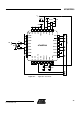
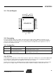
9. Application Circuit
An application circuit with a single-ended RF connector is shown in Figure 9-1. An SMD-balun transforms the
100Ω differential RF inputs/outputs of the AT86RF230 to a 50Ω single ended RF port. The capacitors C1 and C2
form a DC-block.
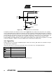
Power supply decoupling capacitors (CB2, CB4) are connected to the analog (28) and the digital supply pin (15).
Capacitors CB1 and CB3 are load capacitors for the analog and digital voltage regulators. They ensure a stable
operation of the low-voltage parts of the AT86RF230. All decoupling capacitors should be placed as close as
possible to the AT86RF230 pin and need to have a low-resistance and low-inductive connection to ground to
achieve the best performance.
The crystal (XTAL), the two load capacitors (CX1, CX2), and the internal circuitry connected to pins XTAL1 and
XTAL2 form the crystal oscillator. To achieve the best accuracy and stability of the reference frequency, large stray
capacitances should be avoided.
Cross coupling of digital signals to the crystal pins or the RF pins can degrade system performance.
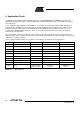
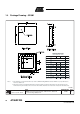
Designator
Description Value Manufacturer Manuf. Part Number
B1 SMD balun 2.4 GHz Wuerth 748421245
CB1 DC-blocking capacitor
1 µF
CB2 DC-blocking capacitor
1 µF
CB3 DC-blocking capacitor
1 µF
CB4 DC-blocking capacitor
1 µF
CX1 Crystal load capacitor 12 pF
CX2 Crystal load capacitor 12 pF
C1 RF-coupling capacitor 22 pF
C2 RF-coupling capacitor 22 pF
XTAL Crystal CX-4025 16 MHz
SX-4025 16 MHz
ACAL Taitjen
Siward
XWBBPL-F-1
A207-011
Table 9-1. Bill of Materials