
Manual


40
AT84AD004
5390A–BDC–06/04
Calibration Description The AT84AD004 offers the possibility of reducing offset and gain matching between the
two ADC cores. An internal digital calibration may start right after the 3-wire serial inter
-
face has been loaded (using data D12 of the 3-wire serial interface with address 000).
The beginning of calibration disables the two ADCs and a standard data acquisition is
performed. The output bit CAL goes to a high level during the entire calibration phase.
When this bit returns to a low level, the two ADCs are calibrated with offset and gain and
can be used again for a standard data acquisition.
If only one channel is selected (I or Q) the offset calibration duration is divided by two
and no gain calibration between the two channels is necessary.
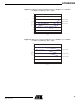
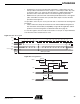
Figure 41. Internal Timing Calibration
The Tcal duration is a multiple of the clock frequency ClockI (master clock). Even if a
dual clock scheme is used during calibration, ClockQ will not be used.
The control wait bits (D13 and D14) give the possibility of changing the calibration’s set-
ting depending on the clock’s frequency:
• For high clock rates (= 500 Msps) use a = b = 1, Tcal = 10112 clock I periods.
• For clock rates > 250 Msps and < 500 Msps use a = 1, b = 0, Tcal = 6016 clock I
periods.
• For clock rates > 125 Msps and < 250 Msps use a = 0, b = 1 ,Tcal = 3968 clock I
periods.
• For low clock rates (< 125 Msps) use a = 0, b = 0 , Tcal = 2944 clock I periods.
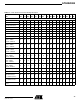
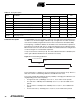
Table 12. Timing Description
Name Parameter
Value
Unit
Min Typ Max
Tsclk Sclk period 20 ns
Twsclk High or low time of sclk 5 ns
Tssldn Setup time of sldn before rising edge of sclk 4 ns
Thsldn Hold time of sldn after rising edge of sclk 2 ns
Tssdata Setup time of sdata before rising edge of sclk 4 ns
Thsdata Hold time of sdata after rising edge of sclk 2 ns
Twlmode Minimum low pulse width of mode 5 ns
Tdmode
Minimum delay between an edge of mode and the
rising edge of sclk
10 ns
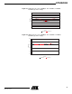
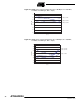
3-wire Serial Interface
LDN
CAL
Tcal