
Manual

23
AT84AD004
5390A–BDC–06/04
Typical Characterization Results
Nominal conditions (unless otherwise specified):
•V
CCA
= 3.3V; V
CCD
= 3.3V; V
CCO
= 2.25V
•V
INI
- V
INB
or V
INQ
to V
INQB
= 500 mVpp full-scale differential input
• LVDS digital outputs (100Ω)
• TA (typical) = 25°C
• Full temperature range: 0
°C < TA < 70°C (commercial grade)
or -40
°C < TA < 85° C (industrial grade)
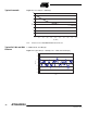
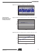
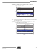
Typical Full Power Input
Bandwidth
• Fs = 500 Msps
• Pclock = 0 dBm
•Pin = -1 dBFS
• Gain flatness (±5 dB) from DC to > 400 MHz
• Full power input bandwidth at -3 dB > 1 GHz
Figure 15. Full Power Input Bandwidth
-7
-6
-5
-4
-3
-2
-1
0
250 500 750 1000 1250 1500
Fin (MHz)
dBFS
-3 dB BandwidthGain Flatness