
Owner manual


9
AT84AD001B
2153C–BDC–04/04
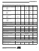
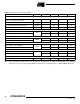
Notes: 1. Differential input [-1 dBFS analog input level], gain setting is 0 dB, two input clock signals, no standby mode,
1:1 DMUX, ISA = -50 ps.
2. Measured on the AT84AD001TD-EB Evaluation Board.
Table 5. AC Performances
Parameter Symbol Min Typ Max Unit
AC Performance
Signal-to-noise Ratio
Fs = 1 Gsps Fin = 20 MHz
SNR
42 44 dBc
Fs = 1 Gsps Fin = 500 MHz 40 42 dBc
Fs = 1 Gsps Fin = 1 GHz 41 dBc
Effective Number of Bits
Fs = 1 Gsps Fin = 20 MHz
ENOB
77.2 Bits
Fs = 1 Gsps Fin = 500 MHz 6.5 6.8 Bits
Fs = 1 Gsps Fin = 1 GHz 6.2 Bits
Total Harmonic Distortion (First 9 Harmonics)
Fs = 1 Gsps Fin = 20 MHz
|THD|
48 54 dBc
Fs = 1 Gsps Fin = 500 MHz 45 51 dBc
Fs = 1 Gsps Fin = 1 GHz 42 dBc
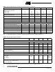
Spurious Free Dynamic Range
Fs = 1 Gsps Fin = 20 MHz
|SFDR|
50 56 dBc
Fs = 1 Gsps Fin = 500 MHz 48 54 dBc
Fs = 1 Gsps Fin = 1 GHz 43 dBc
Two-tone Inter-modulation Distortion (Single Channel)
F
IN1
= 499 MHz , F
IN2
= 501 MHz at Fs = 1 Gsps IMD -54 dBc
Band flatness from DC up to 600 MHz ±0.5 dB
Phase matching using auto-calibration and FiSDA
in interlace mode (channel I and Q)
Fin = 250 MHz
Fs = 1 Gsps
dϕ -0.7 0 0.7 °
Crosstalk channel I versus channel Q
Fin = 250 MHz, Fs = 1 Gsps
(2)
Cr -55 dB