
User guide

65
7511B–SCR–10/05
AT83C26
Electrical Characteristics
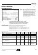
Absolute Maximum Ratings
*
(**) Exposed die attached pad must be soldered to ground
Thermal resistor is measured on multi-layer PCB with 0 m/s air flow.
(***) including shortages between any groups of smart card pins.
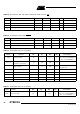
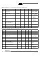
AC/DC Parameters EVCC connected to host power supply: from 2.5V to 5.5V.
T
A
= -40°C to +85°C; V
SS
= 0V; V
CC
= 3V to 5.5V.
CLASS A (5V) for smart card 1, 2, 3, 4, 5 supplied with CVCC (+/- 8%)
CLASS B (3V)for smart card 1, 2, 3, 4, 5 supplied with CVCC (+/- 8%)
CLASS C (1.8V) for smart card 1, 2, 3, 4, 5 supplied with CVCC (+/- 8%)
Ambient Temperature Under Bias: ....................- 40°C to 85°C
Storage Temperature:................................... -65°C to +150°C
Voltage on VCC: ........................................ V
SS
-0.5V to +6.0V
Voltage on SCIB pins (***): .........CVSS
-0.5V to CVCC + 0.5V
Voltage on host interface pins:.......VSS
-0.5V to EVCC + 0.5V
Voltage on other pins:...................... VSS
-0.5V to VCC + 0.5V
Max Power Dissipation: .............................................. 350mW
Thermal resistor of QFN package (**)......................24°C/W
Thermal resistor of VQFP package...........................67°C/W
*NOTICE: Stresses at or above those listed under “Absolute
Maximum Ratings” may cause permanent dam-
age to the device. This is a stress rating only and
functional operation of the device at these or any
other conditions above those indicated in the
operational sections of this specification is not
implied. Exposure to absolute maximum rating
conditions may affect device reliability.
Power Dissipation value is based on the maxi-
mum allowable die temperature and the thermal
resistance of the package.
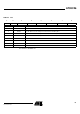
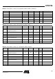
Table 47. Core (VCC)
Symbol Parameter Min Typ Max Unit Test Conditions
V
PFDP
Power fail high level threshold 2.46 2.59 2.71 V
V
PFDM
Power fail low level threshold 2.26 2.40 2.56 V
Hysteresis Delta between (VPFDP - VPFDM) 100 190 300 mV
t
rise
VCC
rise time 1us 10s µs
t
fall
VCC
fall time 100us 10s
I
cc operating
Operating current 15 mA
DCDCA, DCDCB and
LDOs on
with load= 0 mA
VCC = 5.5V
I
cc power down
Power down current 30 µA
SHUTDOWNA bit = 1
SHUTDOWNB bit = 1
VCC = 5.5V