Features • 5 Smart Card Interfaces • • • • • • • • – Compliance with ISO 7816, EMV2000, GIE-CB and GSM Standards – Direct Connection to the Smart Cards Logic Level Shifters Short Circuit Current Limitation 4kV+ ESD Protection (MIL/STD 883 Class 3) – 1 or 2 Master Smart Card interfaces Synchronous Card support (with C4 and C8 Contacts) Card Detection and Automatic de-activation sequence on card extraction – 1 to 4 SAM/SIM cards (15 to 30mA each) – Programmable Voltage for each smart card Class A: 5V ±0.
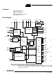
Acronyms TWI: Two Wire Interface POR: Power On Reset PFD: Power Fail Detect ART: Automatic Reset Transition ATR: Answer To Reset Block Diagram VCC VSS CVSSB CVCCB CVCCINB LIB LIA CVSS1 CVCCIN1 DC/DC Converter A BYPASS DC/DC Converter B Voltage supervisor POR/PFD EVCC RESET CVCC1 LDO CVCC2 LDO CVCC3 LDO CVCC4 LDO CVCC5 INT A2/CK, A1/RST CPRES1 SCL TWI Controller SDA CRST1 Main Control & Logic Unit smart card 1 Timer 16 bits CIO1 SC1 CC41 CC81 CCLK1 CPRES2 CRST2 smart card 2 I/O1 I
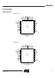
AT83C26 Pin Description Pinout (Top View) CIO2 CCLK2 CRST2 CVCC2 CVCCINB CPRES2 RESET CVCCB CVCCB LIB CVSSB EVCC VQFP48 Pinout 48 47 46 45 44 43 42 41 40 39 38 37 36 1 2 INT CLK A2/CK 33 A1/RST 32 AUX1 31 AUX2 30 IO1 29 IO2 28 SCL 27 SDA 26 BYPASS 25 VSS 35 34 3 4 5 6 VQFP 48 TOP VIEW 7 8 9 10 VCC 11 12 13 14 15 16 17 18 19 20 21 22 23 24 CC81 CC41 CIO1 CCLK1 CRST1 CVCCIN1 CPRES1 CVCC1 CVCC1 LIA CVSS1 CVCC3 CRST3/CC82 CCLK3 CIO3/CC42 CVCC4 CRST4 CCLK4 CIO4 CIO5 CCLK5 CRST5 CVCC5 CIO2 CCLK2 CRST
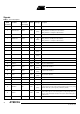
Signals Table 1. Ports Description VQFP48 or QFN48 Pad Name Pin number Pad Internal ESD Limits Pad Type 4kV+ PWR Description Power Supply 1 CVCC3 2 CRST3/CC82 CVCC3 4kV+ 3 CCLK3 CVCC3 4kV+ 4 CIO3/CC42 CVCC3 4kV+ 5 CVCC4 6 CRST4 7 I/O pull up O I/O pull up VCC pin for SC3 interface. See SC2_CFG1 register: If SC2_FULL bit = 0, CRST pin for SC3 interface. If SC2_FULL bit = 1, CC8 pin for SC2 interface. CCLK pin for SC3 interface.
AT83C26 Table 1. Ports Description (Continued) VQFP48 or QFN48 Pad Name Pin number Pad Internal ESD Limits Pad Type Description Power Supply DC/DCA input. LIA must be tied to VCC pin through an external coil (typically 10µH) and provides the current for the charge pump of the DC/DCA converter. 22 LIA 2kV PWR 23 CVSS1 2kV GND 24 VCC 2kV PWR VCC is used to power the internal voltage regulators and I/O buffers. 25 VSS 2kV GND Ground.
Table 1. Ports Description (Continued) VQFP48 or QFN48 Pad Name Pin number 38 Pad Internal ESD Limits Pad Type Description Power Supply CVSSB GND DC/DCB input. This pin must be directly connected to the VSS of power supply. DC/DCB input. 39 LIB 2kV PWR LIB must be tied to VCC pin through an external coil (typically 10µH) and provides the current for the charge pump of the DC/DCB converter.
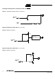
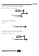
AT83C26 Pad Type Description To simplify the understanding of Figure 1. to Figure 8., a shortcut is possible by replacing the weak transistor by a 100k Ohms pull-up resistor, the medium transistor by a 10k Ohms pull-up resistor and the strong transistor by a 1k Ohms pull-up resistor. Input/Output with Pull-up Configuration (IO1, IO2, AUX1, AUX2) This output type can be used as both an input and output without the need to reconfigure the port.
Input/Output with Open Drain Configuration (SDA, SCL, RESET) Figure 3. Input/Output with Open Drain Configuration Pin N Port latch Data NMOS Input Data Output Configuration (CCLKn with n = 1, 2, 3, 4, 5) Figure 4. Output Configuration P Strong PMOS Slew control with CIOn_SLEW_CTRL bits Pin N Port latch Data NMOS Output Configuration (CRSTn with n = 1, 2, 3, 4, 5) Figure 5.
AT83C26 Open drain Output with programmable pull-up Configuration (INT) Figure 6. Open Drain Output with programmable pull-up P Weak INT_PULLUP bit Pin N Port latch Data NMOS Input Configuration (A1, A2, CLK, BYPASS) Figure 7. Input Input Data Pin Input with programmable pull-up Configuration (CPRES1, CPRES2) Figure 8.
Operational Modes TWI Bus Control The Atmel Two-wire Interface (TWI) interconnects components on a unique two-wire bus, made up of one clock line and one data line with speeds of up to 400 Kbits per second, based on a byte-oriented transfer format. The TWI-bus interface can be used: – To configure the AT83C26 – To select interface – To select the operating mode of the card: 1.
AT83C26 Figure 1. Data transfer on TWI bus SDA acknowledgement from slave command and/or data Address byte SCL 1 2 3 4 5 7 6 8 9 start condition Address Byte stop condition The first byte to send to the device is the address byte. The device controls if the hardware address (A2/CK, A1/RST pins on reset) corresponds to the address given in the address byte (A2, A1 bits). If the level is not stable on A2/CK pin at reset, the user has to manage the possible address taken by the device.
RESET pin The TWI ADDRESS BYTE is sampled on A2/CK and A1/RST after a rising edge on RESET pin. The delay between the rising edge and the sampling of A2/CK and A1/RST is t1. The value for t1 is 22 CLK period. The minimum value for t2 is 40 CLK period. During the t2 time, the TWI bus is not ready to receive a command. The CLK period depends on the frequency of the signal on CLK pin. The RESET pin is an I/O with Open Drain.
AT83C26 Table 3. SC2 and SC3 shared IOs Pin name SC2_FULL = 1 SC3 interface not available SC2_FULL = 0 SC2 without CC4and CC8 + SC3 interface CPRES2 CPRES2 CPRES2 CRST2 CRST2 CRST2 CIO2 CIO2 CIO2 CCLK2 CCLK2 CCLK2 CRST3/CC82 CC82 CRST3 CIO3/CC42 CC42 CIO3 CCLK3 unused CCLK3 DCDC Converters The DC/DC A converter is used to provide smart card voltage for the SC1 interface (CVCC1). The DC/DC B converter is used to provide smart card voltage for the SCn interfaces (n=2, 3, 4, 5).
Figure 4. Clock Block Diagram with Software Activation Internal oscillators CLK DC/DCA and B DCCLK DCK[2:0] CKSn[2:0] A2/CK 0 CARDCKn bit CCLKn 1 CKSTOPn bit CRST controller CRSTn for SCn interface (n=1, 2) The CRSTn output pin is driven by the CARDRSTn bit value or by A1/RST pin. Three modes are available: • If the ARTn bit is reset, CRSTn pin is driven by CARDRSTn bit.
AT83C26 CRSTn for SCn interface (n= 3, 4, 5) The CRSTn output pin is driven by the CARDRSTn bit value (see SCn_CFG2 register). Two modes are available: • If the ARTn bit is reset, CRSTn pin is driven by CARDRSTn bit. • If the ARTn bit is set, CRSTn pin is controlled and follows the “Automatic Reset Transition” (see Activation sequence page 25). Figure 6. CRSTn Block Diagram CARDRSTn bit 0 CRSTn CARDRSTn bit 1 tb delay ARTn bit If SC2_FULL=1, the SC3 interface is not available.
CIO2, CC42, CC82 controller for SC2 interface Figure 8. CIO2, CC42, CC82 Block Diagram 0 CARDIO2 bit IO1 IO2 AUX1 AUX2 HiZ control 1 0 Multiplex CARDC42 bit IODIS2 bit CC42 1 0 CARDC82 bit CIO2 CC82 1 IOSEL[3:0] The SC2_FULL bit must be set to use CC42 and CC82. CIOn controller for SCn interface (n=3, 4, 5) The CIOn output pin is driven by CARDIOn bit values or by I/O1, I/O2, AUX1 or AUX2 signals. This selection depends of the IODISn bit value.
AT83C26 Transparent mode arbitration system The first between IO and CIO to force a low level becomes the master. The slave signal is grounded after t1 delay: t1 max = 2* (CLK period). Figure 10. Bidirectional mode IO master slave t2 CIO slave master t1 t1 t1 t1 The minimum delay for a pulse at 0 or 1 to be detected is between 0.5 and 1.5 CLK period (depending on arrival time). If IO and CIO are both grounded, CIO becomes the master.
CCLKn and CIOn (n=1 to 5) slew rate control Three registers SLEW_CTRL_1, SLEW_CTRL_2 and SLEW_CTRL_3 control the slew rate of the CIOn and CCLKn signals. Each signal has 2 control bits. An automatic mode is proposed. The VCARDn[1:0] value is used to automatically adjust the slew rate. For specific cases, like long wires between AT83C26 and smart card connector for example, the user can forced the slew rate. The rising edge and the falling edge are modified with the slew rate control for CCLKn.
AT83C26 Card Presence Detection Card presence detection for SC1 interface The card presence signal is connected on the CPRES1 pin. The polarity of card presence contact is selected with the CARDDET1 bit (see SC1_CFG1 register). A programmable filtering is controlled with the CDS1[2-0] bits. The internal pull-up on the CPRES1 pin can be disconnected in order to reduce the consumption. An external pull-up must be connected to Vcc. The PULLUP1 bit (see SC1_CFG1 register) controls this feature. Figure 12.
DC/DC converters DC/DC A converter The DC/DC A converter is controlled by VCARD1[1:0], SHUTDOWNA, ICCADJA, STEPREGA, VCARD_OK1 and DEMBOOSTA[1:0] bits. The DC/DC A converter cannot be switched on while the CPRES1 pin remains inactive. If CPRES1 pin becomes inactive while the DC/DC A converter is operating an automatic shut down sequence of the DC/DC A converter is initiated by the electronics. A write operation in VCARD1[1:0] (0x01, 0x02, 0x03) starts the DC/DC.
AT83C26 Figure 9. DC/DC A Converter Initialization Procedure DEMBOOSTA[1:0]=[0:0] Set Time-out to 3 ms VCARD_OK1=1 Time-out Expired Decrement DEMBOOSTA[1:0] to adjust the current overflow END Increment DEMBOOSTA[1:0] DEMBOOSTA[1:0] is at Maximum? DC/DC A Converter Initialization Failure END DC/DC B converter The DC/DC B converter is controlled by DCDCB register. The DC/DC B converter can be switched on even if CPRES2 pin remains inactive.
The DC/DCB sensitivity to any overflow current can be modified (20%) by using the ICCADJB bit (DC/DCB register). Initialization Procedure for DC/DC B converter The initialization procedure is described in flow chart: • Select the DC/DC B level by means of bits VDCB[1:0] in DCDCB register, • Set bits DEMBOOSTB[1:0] in INTERFACEB register following the current level control wanted. • Monitor VDCB_OK bit in DCDCB register in order to know when the DC/DC B Converter is ready Figure 10.
AT83C26 LDO initialization Procedure When the DC/DC B voltage rises the selected voltage (VDCB_OK=1), the card voltage selection on CVCC2, CVCC3, CVCC4 or CVCC5 starts the corresponding LDO. The CVCC2 card voltage must be started in first (if needed). When the VCARD_OK2 is set, the CVCC3,CVCC4, CVCC5 card voltage are started one after each other (if needed) with the same procedure. The SC2_FULL bit must be set to use SC2 full interface: CIO3/CC42 is CC42 and CRST3/CC82 is CC82.
Activation Sequence Overview (n=1, 2, 3, 4, 5) The activation sequence on SC1 is only available if a card is detected on CPRES1 (CARDIN1 bit = 1). The activation sequence on SC2 is only available if a card is detected on CPRES2 (CARDIN2 bit = 1). The activation sequence on SC3, SC4, SC5, is only available if DC/DC B is started (VDCB_OK = 1). The SCn interface starts the activation sequence after a TWI write command in VCARDn[1:0] bits to program the CVCCn voltage.
AT83C26 Figure 14. Software activation without automatic control (ARTn bit = 0) CVCCn CRSTn 4 1 3 CCLKn CIOn ATR 2 Note: – It is assumed that initially VCARDn[1:0], CARDCKn, CARDIOn and CARDRSTn bits are cleared, CKSTOPn and IODISn are set (those bits are further explained in the registers description) – The user should check the AT83C26 status and possibly resume the activation sequence if one TWI transfer is not acknowledged during the activation sequence.
the CRSTn signal is not set and the CAPTURE_MSB and CAPTURE_LSB registers contain the value of the counter at the arrival of the ATR. If the ATR arrives after the rising edge on CRSTn pin and before the card clock counter overflows (65535 clock cycles), the activation sequence completes. The CAPTURE_MSB and CAPTURE_LSB registers contain the value of the counter at the arrival of the ATR (tc time on Figure 15). Figure 15.
AT83C26 The CRST signal will be equal to 0 during the number of clock cycles programmed in TIMER_MSB and TIMER_LSB. Then, the CRST signal will be at 1. Figure 16. Warm reset with ARTn bit = 1 ART = 1 CVCCn CRSTn CCLKn CIOn t t = TIMER value Deactivation Sequence Overview The deactivation sequence should follows the order defined in ISO7816-3 specification.
• Reset pin going low (SC1, SC2, SC3, SC4, SC5) • Power Fail (VPFDP) It is a self-timed sequence which cannot be interrupted when started (see Figure 17). Each step is separated by a delay based on Td equal to 8 periods of DCCLK, typically 2 to 2.4 µs: 1. T0: CARDRSTn is cleared, SHUTDOWNA (for SC1) bit is set. 2. T0 + 5 x Td:CARDCKn is cleared, CKSTOPn, CARDIOn and IODIS are set. 3. T0 + 6 x Td: CARDIOn is cleared. 4. T0 + 7 x Td: VCARDn[1:0] = 00. Figure 17.
AT83C26 Figure 18. Power Fail Detection VCC start standard deactivation VPFDP VPFDM start emergency deactivation Figure 19. Emergency deactivation sequence CVCC CRST CCLK CIO, CC4, CC8 During an emergency deactivation, the signals fall according to the order described in Fig18.
Figure 20. Transparent Mode Description AT83C26 Micro controller CCLK A2/CK CCLKn CRST A1/RST CRSTn CIO I/O1 CIOn CC4 AUX1 CC4n CC8 AUX2 CC8n SMART CARD Full transparent mode on SCn interfaces (n= 3, 4, 5) The transparent mode with A2/CK is also available for SC3, SC4 and SC5 interfaces without CC4 and CC8. Figure 21. Transparent Mode Description AT83C26 Micro controller CCLK A2/CK CCLKn CRSTn CIO I/O2 SIM/SAM CIOn Interrupts The INT output is High by default.
AT83C26 Several AT83C26 devices can share the same interrupt pin and the micro controller can identify the interrupt sources by polling the interrupt bits of the AT83C26 devices using TWI commands. A TWI read command of the interrupt bit corresponding to the IT clears the bit. When all IT bits are cleared, the INT output becomes high. The ITDIS register contains 4 bits to control SCn interrupts (n= 2,3,4,5).
After the reading and the clear of the interrupt bits, several bits are used to control the status. Table 5.
AT83C26 Write Commands The write commands are: 1. General Call Reset: A general call followed by the value 06h has the same effect as a Reset command. 2. Reset: Initialize all the logic and the TWI interface as after a power-up or power-fail reset. If the interface is activated, an emergency de-activation sequence is also performed. This is a one-byte command. 3.
10. Write SC5 interface: SC5_CFG0, SC5_CFG2 Configuration of SIM/SAM interface 5. 11. Write DCDCB config: DCDCB, LDO Configuration of DCDCB converter. 12. Write SLEW_CTRL config: SLEW_CTRL_1, SLEW_CTRL_2, SLEW_CTRL_3 Configuration of slew rate for CCLKn and CIOn (n = 1, 2, 3, 4, 5). Table 6. Write Commands Description Address Byte (See Table 2) Command Byte [0] Data Byte 1 Data Byte 2 [1] Data Byte 3 [2] [3] 1. General Call Reset 0000 0000 0000 0110 2. Reset 0100 XX10 1111 1111 3.
AT83C26 Read Command After a write command, even with a length of 0 byte, the next read operation is performed on the corresponding byte. The write command sets the “read pointer”. After the reset, the “read pointer” is on SC1 registers FFh is completing the transfer if the micro controller attempts to read beyond the last byte. Flags are only reseted after the corresponding byte read has been acknowledged by the master. Figure 23.
Registers summary The table below gives a quick view on AT83C26 registers. Table 8.
AT83C26 Table 13. Common registers for SC1/SC2/SC3/SC4/SC5 7 6 5 4 3 2 1 0 TIMER_MSB Bit 15 Bit 14 Bit 13 Bit 12 Bit 11 Bit 10 Bit 9 Bit 8 TIMER_LSB Bit 7 Bit 6 Bit 5 Bit 4 Bit 3 Bit 2 Bit 1 Bit 0 CAPTURE_MSB Bit 15 Bit 14 Bit 13 Bit 12 Bit 11 Bit 10 Bit 9 Bit 8 CAPTURE_LSB Bit 7 Bit 6 Bit 5 Bit 4 Bit 3 Bit 2 Bit 1 Bit 0 X X X X IOSEL3 IOSEL2 IOSEL1 IOSEL0 IO_SELECT Table 14.
Registers Table 17. SC1_ CFG0(Config Byte 0 for SC1) 7 6 5 4 3 2 1 0 1 0 ATRERR1 INSERT1 ICARDERR1 VCARDERR1 VCARD11 VCARD10 Bit Number Bit Mnemonic 7-6 1-0 Description These bits cannot be programmed and are read as 1-0. Answer to Reset Interrupt for SC1 5 ATRERR1 This bit is set when the card clock counter overflows (no falling edge on CIO1 is received before the overflow of the card clock counter). This bit is cleared by hardware when this register is read.
AT83C26 SC1_CFG Table 18. SC1_CFG1 (Config Byte 1 for SC1 7 6 5 4 3 2 1 0 X ART1 SHUTDOWNA CARDDET1 PULLUP1 CDS12 CDS11 CDS10 Bit Number Bit Mnemonic 7 X 6 ART1 Description Automatic Reset Transition Set this bit to have the CRST1 pin changed according to activation sequence. Clear this bit to have the CRST1 pin immediately following the value programmed in CARDRST1. Shutdown DC/DCA 5 SHUTDOWNA Set this bit to reduce the power consumption.
Table 19. SC1_CFG2 (Config Byte 2 for SC1) 7 6 5 4 3 2 1 0 0 DCK2 DCK1 DCK0 X CKS12 CKS11 CKS10 Bit Number Bit Mnemonic 7 0 Description This bit must be always at 0. DCK is the first level of prescaler factor. CLK signal is divided by the prescaler value and outputs DCCLK signal. DCCLK is an input for CCLK prescaler.
AT83C26 Table 20. SC1_CFG3 (Config Byte 3 for SC1) 7 6 5 4 3 2 1 0 X X X ICCADJA X X X X Bit Number Bit Mnemonic 7-5 X Description CICC overflow adjust This bit controls the DC/DCA sensitivity to any overflow current. 4 ICCADJA Set this bit to decrease the DC/DCA sensitivity (CICC_ovf is increased by about 20%). Clear this bit to have a normal configuration. The reset value is 0.
Table 21. SC1_CFG4 (Config Byte 4 for SC1) 7 6 5 4 3 2 1 0 X DEMBOOSTA1 DEMBOOSTA0 STEPREGA INT_PULLUP X X CRST_SEL1 Bit Number Bit Mnemonic 7 X Description DC/DC A Maximum Startup Current drawn from power supply 00: Normal: 80 mA average 6-5 DEMBOOSTA[1-0] 01: Normal + 18% 10: Normal + 18% (and boost on oscillator) 11: Normal + 40% 4 STEPREGA Step Regulator mode Clear this bit to enable the automatic step-up converter (CVCC is stable even if VCC is not higher than CVCC).
AT83C26 _ Table 22. SC1_INTERFACE (Interface Byte for SC1) 7 6 5 4 3 2 1 0 0 IODIS1 CKSTOP1 CARDRST1 CARDC81 CARDC41 CARDCK1 CARDIO1 Bit Number 7 Bit Mnemonic 0 Description This bit should not be set. Card I/O isolation 6 IODIS1 Set this bit to drive the CIO1, CC41, CC81 pins according to CARDIO1, CARDC41, CARDC81 respectively. Clear this bit to drive the CIO1, CC41 and CC81 pins connected to inputs according to IOSEL[3/0] bits.
Table 23. SC1_STATUS (Status Byte for SC1) 7 6 5 4 3 2 1 0 CC81 CC41 CARDIN1 VCARD_OK1 X VCARD_INT1 CRST1 CIO1 Bit Number Bit Mnemonic 7 CC81 Card CC8 This bit provides the actual level on the CC8 pin when read. 6 CC41 Card CC4 This bit provides the actual level on the CC4 pin when read. 5 CARDIN1 4 VCARD_OK1 3 X 2 VCARD_INT1 Description Card Presence Status This bit is set when a card is detected. It is cleared otherwise.
AT83C26 Table 24. SC2_CFG0 () 7 6 5 4 3 2 1 0 VCARD_INT 2 VCARD_OK 2 ATRERR2 INSERT2 X VCARDERR2 VCARD21 VCARD20 Bit Number Bit Mnemonic 7 VCARD_INT2 Description SC2 voltage interrupt This bit is set when VCARD_OK2 bit is set. This bit is cleared when read by the micro controller. 6 VCARD_OK2 SC2 Voltage Status This bit is set by the LD02 when the output voltage remains within the voltage range specified by VCARD2[1:0] bits. It is cleared otherwise.
Table 25. SC2_CFG1 () 7 6 5 4 3 2 1 0 X X SC2_FULL CARDDET2 PULLUP2 CDS22 CDS21 CDS20 Bit Number Bit Mnemonic 7-6 X Description Set this bit to activate full IO interface on Smart card 2: • 5 SC2_FULL CIO3/CC42 is CC42 and CRST3/CC82 is CC82. • Interface 3 LDO is disabled. • CARDCK3 is reset and CKSTOP3 to stop CCLK on SC3. • ITDIS3 is set to disable interrupts from SC3. CVCC2 and CVCC3 shall be connected externally and SC2_FULL must be set before activating the LDO.
AT83C26 Table 26. SC2_CFG2 () 7 6 5 4 3 2 1 0 ART2 CRST_SEL2 CARDRST2 CARDCK2 CKSTOP2 CKS22 CKS21 CKS20 Bit Number Bit Mnemonic 7 ART2 Description Automatic Reset Transition Set this bit to have the CRST2 pin changed according to activation sequence. Clear this bit to have the CRST2 pin immediately following the value programmed in CARDRST2. Card Reset Selection 6 CRST_SEL2 Set this bit to have the CRST2 pin driven by hardware through the A1/RST pin.
Table 27. SC3_CFG0() 7 6 5 4 3 2 1 0 VCARD_INT3 VCARD_OK3 ATRERR3 X X VCARDERR3 VCARD31 VCARD30 Bit Number Bit Mnemonic 7 VCARD_INT3 Description SC3 voltage interrupt This bit is set when VCARD_OK3 bit is set. This bit is cleared when read by the micro controller. 6 VCARD_OK3 SC3 Voltage Status This bit is set by the LDO3 when the output voltage remains within the voltage range specified by VCARD3[1:0] bits. It is cleared otherwise.
AT83C26 Table 28. SC3_CFG2 () 7 6 5 4 3 2 1 0 ART3 X CARDRST3 CARDCK3 CKSTOP3 CK32 CKS31 CKS30 Bit Number Bit Mnemonic 7 ART3 Description Automatic Reset Transition Set this bit to have the CRST3 pin changed according to activation sequence. Clear this bit to have the CRST3 pin immediately following the value programmed in CARDRST3. 6 5 X CARDRST3 Card Reset Set this bit to enter a reset sequence according to ART3 bit value. Clear this bit to drive a low level on the CRST3 pin.
Table 29. SC4_CFG0() 7 6 5 4 3 2 1 0 VCARD_INT4 VCARD_OK4 ATRERR4 X X VCARDERR4 VCARD41 VCARD40 Bit Number Bit Mnemonic 7 VCARD_INT4 Description SC4 voltage interrupt This bit is set when VCARD_OK4 bit is set. This bit is cleared when read by the micro controller. 6 VCARD_OK4 SC4 Voltage Status This bit is set by the LD04 when the output voltage remains within the voltage range specified by VCARD4[1:0] bits. It is cleared otherwise.
AT83C26 Table 30. SC4_CFG2 () 7 6 5 4 3 2 1 0 ART4 X CARDRST4 CARDCK4 CKSTOP4 CKS42 CKS41 CKS40 Bit Number Bit Mnemonic 7 ART4 Description Automatic Reset Transition Set this bit to have the CRST4 pin changed according to activation sequence. Clear this bit to have the CRST4 pin immediately following the value programmed in CARDRST4. 6 X 5 CARDRST4 Card Reset Set this bit to enter a reset sequence according to ART4 bit value. Clear this bit to drive a low level on the CRST4 pin.
Table 31. SC5_CFG0() 7 6 5 4 3 2 1 0 VCARD_INT5 VCARD_OK5 ATRERR5 X X VCARDERR5 VCARD51 VCARD50 Bit Number Bit Mnemonic 7 VCARD_INT5 Description SC5 voltage interrupt This bit is set when VCARD_OK5 bit is set. This bit is cleared when read by the micro controller. 6 VCARD_OK5 SC5 Voltage Status This bit is set by the LDO5 when the output voltage remains within the voltage range specified by VCARD5[1:0] bits. It is cleared otherwise.
AT83C26 Table 32. SC5_CFG2 () 7 6 5 4 3 2 1 0 ART5 X CARDRST5 CARDCK5 CKSTOP5 CKS52 CKS51 CKS50 Bit Number Bit Mnemonic 7 ART5 Description Automatic Reset Transition Set this bit to have the CRST5 pin changed according to activation sequence. Clear this bit to have the CRST5 pin immediately following the value programmed in CARDRST5. 6 X 5 CARDRST5 Card Reset Set this bit to enter a reset sequence according to ART5 bit value. Clear this bit to drive a low level on the CRST5 pin.
Table 33. TIMER_MSB (Timer MSB for SC1, SC2, SC3, SC4, SC5) 7 6 5 4 3 2 1 0 Bit 15 Bit 14 Bit 13 Bit 12 Bit 11 Bit 10 Bit 9 Bit 8 Bit Number Bit Mnemonic 7-0 Bits 15 - 8 Description Timer MSB (bits 15 to 8) Reset value = 0x 0000 0001 Table 34. TIMER_LSB (Timer LSB for SC1, SC2, SC3, SC4, SC5) 7 6 5 4 3 2 1 0 Bit 7 Bit 6 Bit 5 Bit 4 Bit 3 Bit 2 Bit 1 Bit 0 Bit Number Bit Mnemonic 7-0 bits 7 - 0 Description Timer LSB (bits 7to 0) Reset value = 0x 1001 0000 Table 35.
AT83C26 Table 37. IO_SELECT (Selection byte for IO) 7 6 5 4 3 2 1 0 X X X X IOSEL3 IOSEL2 IOSEL1 IOSEL0 Bit Number Bit Mnemonic 7 X 6 X 5 X 4 X Description IO Selection 3-0 IOSEL[3:0] This field indicates the IO routing between the host and the Smart Card Interfaces when activated, seeTable 38 and IODISn value (n=1, 2, 3, 4, 5). When no host IO is routed to a smart card pin, this pin is driven according to the Interface register. See Section “CIO, CC4, CC8 controller”, page 15.
Note: 1. If no input (IO1, IO2, AUX1, AUX2) is selected for a SCIB pin (CIOn, CC4n CC8n), and if the smart card interface is started, the electrical level on the SCIB pin corresponds to the CARDIOn, CARDC4n or CARDC8n bit value. 2. For IOSEL[3:0] = 0xOE and IOSEL[3:0] = 0x0F, the CARDRST3 bit must be set to connect AUX2 to CRST3/CC82 pin.
AT83C26 Table 39. INTERFACEB () 7 6 5 4 3 2 1 0 X CARDC82 CARDIO5 CARDIO4 CARDIO3/CAR DC42 CARDIO2 DEMBOOSTB1 DEMBOOSTB0 Bit Number Bit Mnemonic 7 X 6 CARDC82 Description Set this bit to drive the CRST3/CC82 pin High with the on-chip pull-up (according to IODIS2 bit value). The pin can then be an input (read in STATUSB register). Clear this bit to drive a low level on the CC82 pin (according to IODIS2 bit value).
Table 40. STATUSB () - Read Only 7 6 5 4 X CARDIN2 CIO5 CIO4 Bit Number Bit Mnemonic 7 X 6 CARDIN2 5 CIO5 4 CIO4 3 CRST3/CC82 2 CIO3/CC42 1 CRST2 0 CIO2 3 2 CRST3/ CIO3/ CC82 CC42 1 0 CRST2 CIO2 Description Card Presence Status 2 This bit is set when a card is detected. It is cleared otherwise. Card CIO5 This bit provides the actual level on the CIO5 pin when read. Card CIO4 This bit provides the actual level on the CIO4 pin when read.
AT83C26 Table 41. ITDIS () 7 6 5 4 3 2 1 0 IODIS5 IODIS4 IODIS3 IODIS2 ITDIS5 ITDIS4 ITDIS3 ITDIS2 Bit Number Bit Mnemonic Description Card I/O isolation 7 IODIS5 Set this bit to drive CIO5 pin according to CARDIO5. Clear this bit to drive the CIO5 pin connected to inputs according to IO_SELECT registers. If IOSEL config doesn’t link an input to CIO5, CIO5 outputs CARDIO5 value. Card I/O isolation 6 IODIS4 Set this bit to drive CIO4 pin according to CARDIO4.
Table 42. DCDCB (Config Interface B Byte 2) 7 6 SHUTDOWNB Bit Number 5 VDCB_INT Bit Mnemonic VDCB_OK 4 0 3 ICCADJB 2 STEPREGB 1 0 VDCB1 VDCB0 Description Shutdown DCDCB 7 SHUTDOWNB Set this bit to reduce the power consumption. An automatic de-activation sequence will be done. Clear this bit to enable VDCB. The reset value is 0. DC/DC B voltage interrupt 6 VDCB_INT This bit is set when VCARD_OKB bit is set. This bit is cleared when read by the micro controller. The reset value is 0.
AT83C26 Table 43. LDO 7 6 5 4 3 2 1 0 IPLUS5 IPLUS4 IPLUS3 IPLUS2 1 1 1 1 Bit Number Bit Mnemonic Description 7 IPLUS5 If set, this bit increases the startup and overflow current of LDO5 (+60%) 6 IPLUS4 If set, this bit increases the startup and overflow current of LDO4 (+60%) 5 IPLUS3 If set, this bit increases the startup and overflow current of LDO3 (+60%) 4 IPLUS2 If set, this bit increases the startup and overflow current of LDO2 (+60%) 3 1 Do not clear this bit.
Table 44. SLEW_CTRL_1(Slew control for SC1 and SC2) 7 6 5 4 3 2 1 0 CCLK2_SLEW_CT RL1 CCLK2_SLEW_CT RL0 CIO2_SLEW_CT RL1 CIO2_SLEW_CT RL0 CCLK1_SLEW_CT RL1 CCLK1_SLEW_CTR L0 CIO1_SLEW_CTR L1 CIO1_SLEW_CT RL0 Bit Number Bit Mnemonic Description 0 0: Mode 1 (optimum for CVCC2=5V) 0 1: Mode 2 (optimum for CVCC2=3V) 7-6 CCLK2_SLEW_CTRL[1-0] 1 0: Mode 3 (optimum for CVCC2=1.8V) 1 1: Automatic mode The reset value is 11.
AT83C26 Table 45. SLEW_CTRL_2 (Slew control for SC3 and SC4) 7 6 5 4 3 2 1 0 CCLK4_SLEW_CTR L1 CCLK4_SLEW_CT RL0 CIO4_SLEW_CT RL1 CIO4_SLEW_CT RL0 CCLK3_SLEW_CTR L1 CCLK3_SLEW_CTRL 0 CIO3_SLEW_CT RL1 CIO3_SLEW_CTR L0 Bit Number Bit Mnemonic Description 0 0: Mode 1 (optimum for CVCC4=5V) 0 1: Mode 2 (optimum for CVCC4=3V) 7-6 CCLK4_SLEW_CTRL[1-0] 1 0: Mode 3 (optimum for CVCC4=1.8V) 1 1: Automatic mode The reset value is 11.
Table 46. SLEW_CTRL_3 (Slew control for SC5) 7 6 5 4 3 2 1 0 X X X X CCLK5_SLEW_CTR L1 CCLK5_SLEW_CTR L0 CIO5_SLEW_CTR L1 CIO5_SLEW_CT RL0 Bit Number Bit Mnemonic 7-4 X Description 0 0: Mode 1 (optimum for CVCC5=5V) 0 1: Mode 2 (optimum for CVCC5=3V) 3-2 CCLK5_SLEW_CTRL[1-0] 1 0: Mode 3 (optimum for CVCC5=1.8V) 1 1: Automatic mode The reset value is 11. 0 0: Mode 1 (optimum for CVCC5=5V) 0 1: Mode 2 (optimum for CVCC5=3V) 1-0 CIO5_SLEW_CTRL[1-0] 1 0: Mode 3 (optimum for CVCC5=1.
AT83C26 Electrical Characteristics Absolute Maximum Ratings * *NOTICE: Ambient Temperature Under Bias: ....................- 40°C to 85°C Storage Temperature: ................................... -65°C to +150°C Voltage on VCC: ........................................ VSS -0.5V to +6.0V Voltage on SCIB pins (***): ......... CVSS -0.5V to CVCC + 0.5V Voltage on host interface pins:.......VSS -0.5V to EVCC + 0.5V Voltage on other pins: ...................... VSS -0.5V to VCC + 0.
Table 48. Host Interface (IO1, IO2, AUX1, AUX2, CLK, A2/CK, A1/RST, INT) Symbol Parameter VIL Input Low-voltage VIH Input High Voltage VOL Output low voltage VOH Output High Voltage Min Typ Max Unit 0.8 V 2.2 Test Conditions V 0.3 VCC - 0.7V V IOL = -500µA V IOH = +30µA Table 49. Host Interface (SCL, SDA, RESET) Symbol Parameter VIL Input Low-voltage VIH Input High Voltage VOL Output low voltage Min Typ Max Unit 0.8 V 2.2 Test Conditions V 0.
AT83C26 Table 51. Smart Card 1 Class B, 3V (CVCC1) (Continued) Symbol Min Typ Max Unit 70 115 200 mA Ripple on CVCC 60 200 mV Spikes on CVCC 0.4 V 3 V Vcardok low level threshold 2.82 V TVHL CVCC valid to 0.4V 100 400 μs CL =10μF TVLH CVCC 0 to valid 300 2000 μs CL = 10μF CICC_ovf Parameter Card Supply Current Overflow: ICCADJA = 0 (reset value) Vcardok up Vcardok high level threshold Vcardok down Test Conditions With low ESR capacitance (0.1 Ohms max) Table 52.
Table 53. Smart Card 2 Class A, 5V (CVCC2) (Continued) Symbol TVLH Parameter Min CVCC 0 to valid Typ Max Unit 200 2000 μs Test Conditions CL = 2.2μF Table 54. Smart Card 2 Class B, 3V (CVCC2) Symbol CVCC Parameter Min Typ Max Unit Test Conditions Smart card voltage 2.76 3 3.
AT83C26 Table 56. Smart Card 3, 4, 5 Class A, 5V (CVCC3, CVCC4, CVCC5) (Continued) Symbol Parameter Min Ripple on CVCC Typ Max Unit 30 200 mV Spikes on CVCC Test Conditions V Vcardok up Vcardok high level threshold 5 V Vcardok down Vcardok low level threshold 4.65 V TVHL CVCC valid to 0.4V 50 500 μs CL =470nF TVLH CVCC 0 to valid 200 2000 μs CL = 470nF Table 57.
Table 59. Smart Card 1, 2, 3, 4, 5 Clock (CCLK1, CCLK2, CCLK3, CCLK4, CCLK5) Symbol Parameter Min Typ Max Unit 0.3 V Test Conditions Class A: IOL = -200µA VOL Output low voltage Class B: IOL = -200µA Class C: IOL = -200µA Class A: IOH = 200µA VOH Output High Voltage 0.
AT83C26 Table 60. Smart Card n I/Os (CIOn, CC4n, CC8n, CRSTn) (n =1, 2, 3, 4, 5) (Continued) Symbol tF Parameter Min Typ Fall time Max Unit 100 μs Test Conditions CL = 30pF Class A CL = 30pF Class B CL = 30pF Class C Table 61.
Table 64. Slew rate on CIOn with CVCCn= 3V (n=1, 2, 3, 4, 5), Mode 2 Symbol tR/F Parameter Min Rise time/ Fall time with CIOn_SLEW_CTRL[1-0] = 01 (3V) Typ Max Unit 9 ns 4 ns Test Conditions or CIOn_SLEW_CTRL[1-0] = 11(mode auto) tR Rise time with CIOn_SLEW_CTRL[1-0] = 10 (1.8V) Table 65. Slew rate on CIOn with CVCCn= 1.8V (n=1, 2, 3, 4, 5), Mode 3 Symbol tR/F Parameter Min Rise time/ Fall time with CIOn_SLEW_CTRL[1-0] = 10 (1.8V) Typ Max 8.
AT83C26 Typical Application VCC 100nF 4.7µF 10µH 100nF 2.2µF VSS Px.y RESET INT0 CVSS LIA INT Card 1 2.2µF VSS 4 * Px,y IO1,IO2, AUX1, AUX2 CCLK A2/CK CRST0 A1/RST Card 3..5 Card 2 CVSS Px.y LIB BYPASS VSS CLK_OUT CRST3..5 CIO3..5 CCLK3..
Ordering Information Part Number Supply Voltage Temperature Range Package Packing AT83C26-PLTUL 3V to 5.5V Industrial MLF48 Tray AT83C26-PLRUL 3V to 5.5V Industrial MLF48 Tape&Reel AT83C26-RKTUL 3V to 5.5V Industrial VQFP48 Tray AT83C26-RKRUL 3V to 5.5V Industrial VQFP48 Tape&Reel Part Number Supply Voltage Temperature Range Package Packing AT83C26-PLTEL 3V to 5.5V 25°C MLF48 Tray AT83C26-RKTEL 3V to 5.
AT83C26 Package Drawings VQFP48 75 7511B–SCR–10/05
QFN48 76 AT83C26 7511B–SCR–10/05
Atmel Corporation 2325 Orchard Parkway San Jose, CA 95131, USA Tel: 1(408) 441-0311 Fax: 1(408) 487-2600 Regional Headquarters Europe Atmel Sarl Route des Arsenaux 41 Case Postale 80 CH-1705 Fribourg Switzerland Tel: (41) 26-426-5555 Fax: (41) 26-426-5500 Asia Room 1219 Chinachem Golden Plaza 77 Mody Road Tsimshatsui East Kowloon Hong Kong Tel: (852) 2721-9778 Fax: (852) 2722-1369 Japan 9F, Tonetsu Shinkawa Bldg.