
Owner manual

3
AT75C320
1769A–07/01
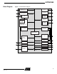
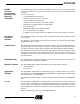
AT75C320 Pin Description
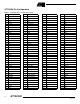
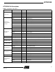
Table 2. AT75C320 Pin Description
Block PQFP Pin Name Type Function
Common Bus
A[21:0] O Address Bus
D[15:0] I/O Data Bus
NREQ I Bus Request
NGNT O Bus Grant
Synchronous
Dynamic Memory
Controller
DCK O SDRAM Clock
DQM[1:0] O Memory Data Byte Masks
CS0 O SDRAM Chip Select
CS1 O SDRAM Chip Select
WE O SDRAM Write Enable
RAS O Row Address Select
CAS O Column Address Select
Static Memory
Controller
NCE0, NCE3 O Chip Selects
NWE[1:0] O Byte Select/Write
NSOE O Enable Output
NWR O Enable Memory Block Write
NWAIT I Enable Enable Wait States
I/O Port A PA[12:0], PA19 I/O General Purpose I/O Lines. Multiplexed with Peripheral I/Os
I/O Port B PB[9:0] I/O General Purpose I/O Lines. Multiplexed with Peripheral I/Os
DSP Subsystem A
OakAIN[1:0] I OakDSPCore A User Inputs
OakAOUT[1:0] O OakDSPCore A User Outputs
DSP Subsystem B
OakBIN[1:0] I OakDSPCore B User Inputs
OakBOUT[1:0] O OakDSPCore B User Outputs
Timer/Counter 0
TCLK0 I Timer 0 External Clock
TIOA0 I/O Timer 0 Signal A
TIOB0 I/O Timer 0 Signal B
Timer/Counter 1
TCLK1 I Timer 1 External Clock
TIOA1 I/O Timer 1 Signal A
TIOB1 I/O Timer 1 Signal B
Watchdog NWDOVF O Watchdog Overflow
Serial Peripheral
Interface
MISO I/O Master In/Slave Out
MOSI I/O Master Out/Slave In
SPCK I/O Serial Clock
NPCSS I/O Chip Select/Slave Select