
Manual

AT75C310
18
• External Wait
The NWAIT input can be used to add wait states at any
time NWAIT is active low and is detected on the rising edge
of the clock. If NWAIT is low at the rising edge of the clock,
the SMC adds a wait state and does not change the output
signals.
• Chip Select Change Wait States
A chip select wait state is automatically inserted when con-
secutive accesses are made to two different external mem-
ories and no wait states have been inserted. If wait states
have been inserted (e.g., data float wait), then none are
added.
LCD Interface Mode
NCE3 can be configured for use with an external LCD con-
troller by setting the LCD bit in the SMC_CSR3 register.
Additionally, WSE must be set and NWS programmed with
a value of 1 or more.
In LCD mode, NCE3 is shortened by one-half clock cycle at
the leading and trailing edges, providing positive address
setup and hold. For read cycles, the data is latched in the
SMC as NCE3 is raised at the end of the access.
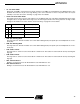
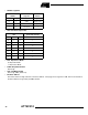
SMC Register Map
The SMC is programmed using the registers listed in Table
8. The memory control register (SMC_MCR) is used to pro-
gram the number of active chip selects and data read pro-
tocol. Four chip select registers (SMC_CSR0 to
SMC_CSR3) are used to program the parameters for the
individual external memories. Each SMC_CSR must be
programmed with a different base address even for unused
chip selects. The AT75C310 resets such that SMC_CSR0
is configured as having a 16-bit data bus.
Table 8. SMC Register Map
Offset Register Description Register Name Access Reset State
0x00
Chip Select Register
SMC_CSR0 Read/write 0x0000203D
0x04
Chip Select Register
SMC_CSR1 Read/write 0x10000000
0x08
Chip Select Register
SMC_CSR2 Read/write 0x20000000
0x0C
Chip Select Register
SMC_CSR3 Read/write 0x30000000
0x10
Reserved
–– –
0x14
Reserved
–– –
0x18
Reserved
–– –
0x1C
Reserved
–– –
0x20
Reserved
–– –
0x24
Memory Control Register
SMC_MCR Read/write 0