
Manual

AT75C310
115
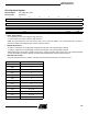
SPI Chip Select Register
Register Name: SP_CSR0..SP_CSR1
Access Type: Read/write
• CPOL: Clock Polarity
0 = The inactive state value of SPCK is logic level zero.
1 = The inactive state value of SPCK is logic level one.
CPOL is used to determine the inactive state value of the serial clock (SPCK). It is used with NCPHA to produce a
desired clock/data relationship between master and slave devices.
• NCPHA: Clock Phase
0 = Data is changed on the leading edge of SPCK and captured on the following edge of SPCK.
1 = Data is captured on the leading edge of SPCK and changed on the following edge of SPCK.
NCPHA determines which edge of SPCK causes data to change and which edge causes data to be captured. NCPHA
is used with CPOL to produce a desired clock/data relationship between master and slave devices.
• BITS: Bits Per Transfer
The BITS field determines the number of data bits transferred. Reserved values should not be used.
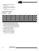
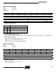
31 30 29 28 27 26 25 24
DLYBCT
23 22 21 20 19 18 17 16
DLYBS
15 14 13 12 11 10 9 8
SCBR
76543210
BITS ––NCPHA CPOL
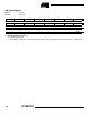
BITS[3:0] Bits per Transfer
0000 8
0001 9
0010 10
0011 11
0100 12
0101 13
0110 14
0111 15
1000 16
1001 Reserved
1010 Reserved
1011 Reserved
1100 Reserved